Self-test design methodology and technique for root-gated clocking structure

Inactive Publication Date: 2010-09-16
MARVELL ASIA PTE LTD
View PDF2 Cites 2 Cited by
  • Summary
  • Abstract
  • Description
  • Claims
  • Application Information

AI Technical Summary

Benefits of technology

[0012]The disadvantages of the prior art are overcome by the present invention which, in one aspect, is a method of generating clock signals for a level-sensitive scan design latch, in which at least one test input signal is transmitted to a plurality of splitter leaves. Once the at least one test input signal is stabilized at each of the splitter leaves, generating a shaped oscillator clock signal having a predetermined pattern of pulses from a central root is generated. At the plurality of splitter leaves, the at least one test input signal is logically combi

Problems solved by technology

Digital integrated circuits sometimes experience faults that interfere with circuit functionality.
Functional testing is effective for simple circuits, but becomes unmanageably complex as the complexity of the circuit grows.
This approach has the disadvantage of being cumbersome and using a considerable amount of chip area.
In LSSD designs that require precise clock control, such as those with Logic Built-In Self-Test (LBIST), it is increasingly challenging to gate the clocks in a physical design and still pass static timing analysis requirements.
With root gating, however, test coverage typically declines due to the lack of unique control at the splitter level.
However, the ASST structures are not available in certain earlier technologies.

Method used


Image

  • Self-test design methodology and technique for root-gated clocking structure
  • Self-test design methodology and technique for root-gated clocking structure
  • Self-test design methodology and technique for root-gated clocking structure

Examples


Embodiment Construction

[0028]A preferred embodiment of the invention is now described in detail. Referring to the drawings, like numbers indicate like parts throughout the views. As used in the description herein and throughout the claims, the following terms take the meanings explicitly associated herein, unless the context clearly dictates otherwise: the meaning of “a,”“an,” and “the” includes plural reference, the meaning of “in” includes “in” and “on.”

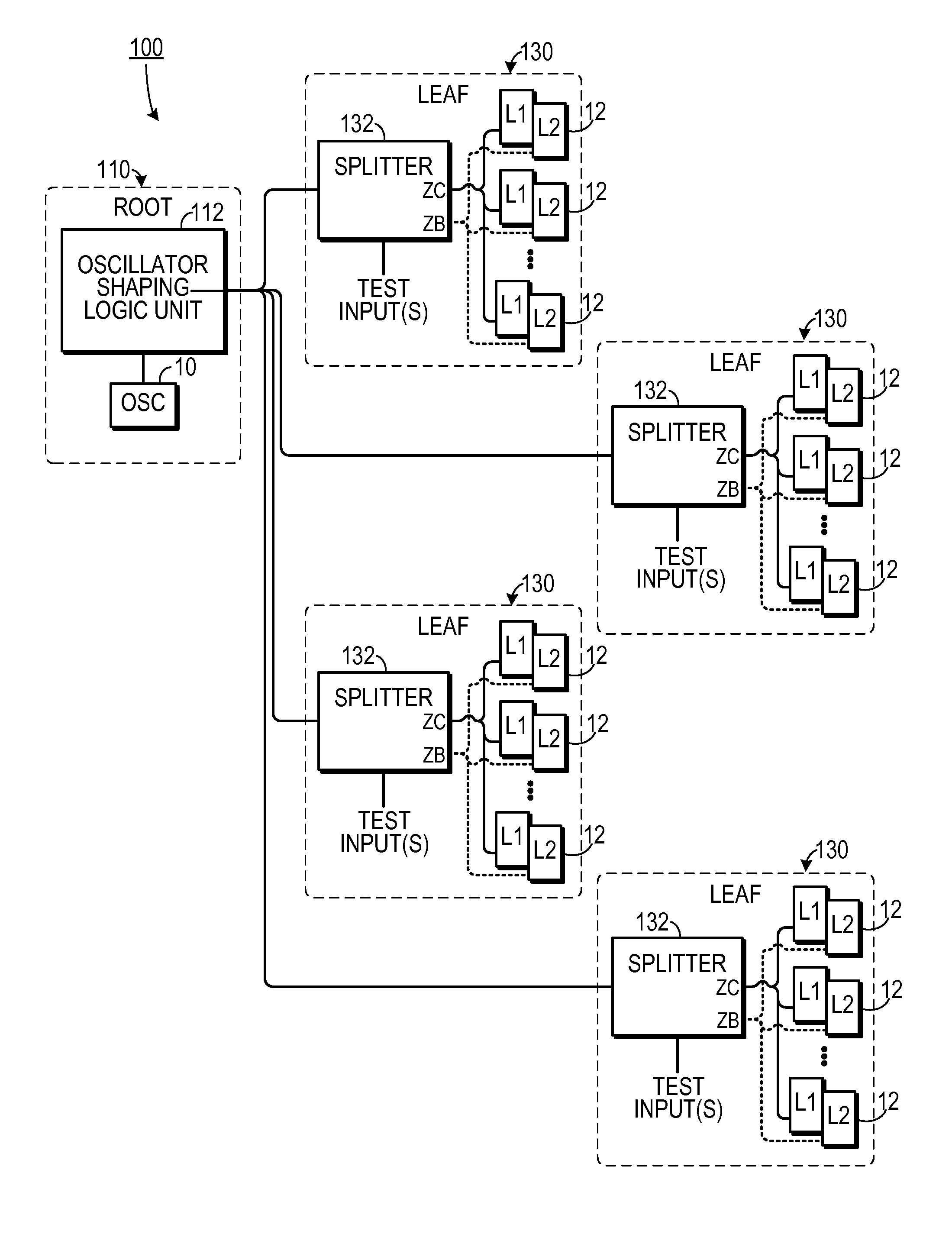
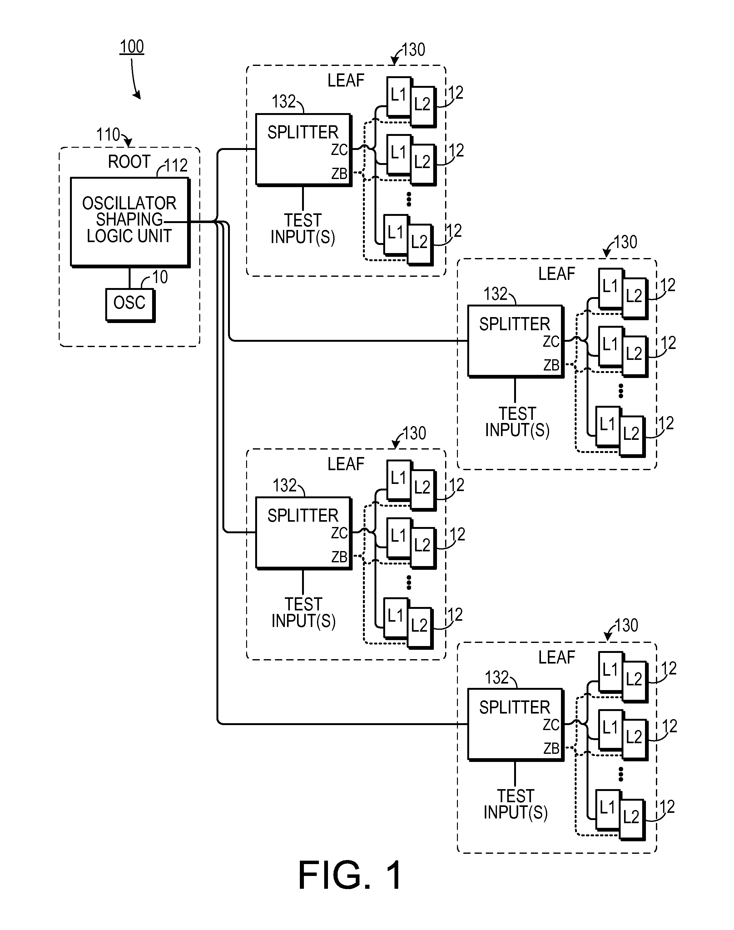
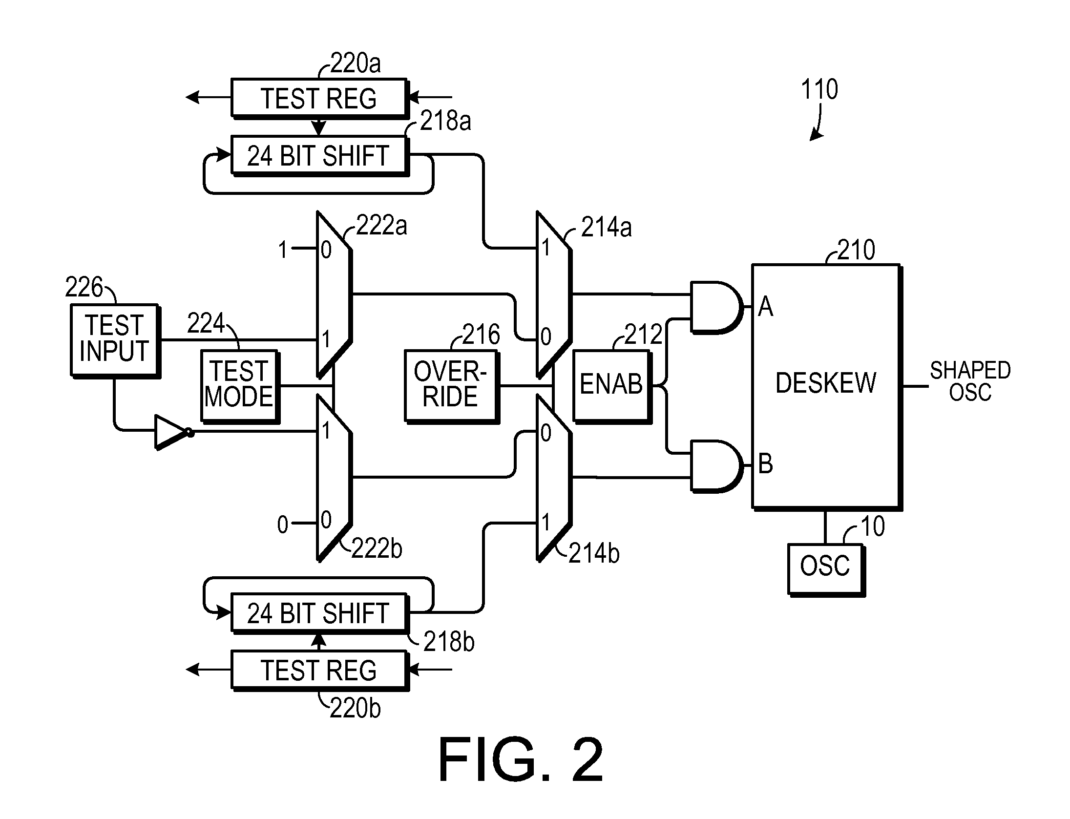
[0029]As shown in FIG. 1, one embodiment employs a root oscillation signal shaping logic circuit 110 that is employed on an integrated circuit, such as a processor. The root oscillation signal shaping logic circuit 110 includes an oscillator 10 that asserts a clock signal and an oscillator shaping logic unit 112 that generates and transmits a shaped oscillator clock signal to a plurality of clock splitter waveform generators 130, also referred to herein as “splitter leaves.” Each splitter leaf 130 includes a clock splitter 132 that generates latch clock ...


PUM


Abstract

In a method of generating clock signals for a level-sensitive scan design latch, at least one test input signal is transmitted to a plurality of splitter leaves. Once the test input signal is stabilized at each of the splitter leaves, generating a shaped oscillator clock signal having a predetermined pattern of pulses from a central root is generated. At the plurality of splitter leaves, the test input signal is logically combined with the shaped oscillator clock signal, thereby generating a first latch clock signal and a second latch clock signal. The logically combining action includes applying a delay of less than one clock cycle to the shaped oscillator clock signal to generate a delayed oscillator clock signal; logically combining the delayed oscillator clock signal with a second signal so as to generate the first latch clock signal; and logically combining the shaped oscillator clock signal with a third signal so as to generate the second latch clock signal.

Description

BACKGROUND OF THE INVENTION[0001]1. Field of the Invention[0002]The present invention relates to self-test circuits used in digital systems and, more specifically, to a clocking system used with a self-test circuit.[0003]2. Description of the Prior Art[0004]Digital integrated circuits sometimes experience faults that interfere with circuit functionality. Most modern digital circuits of any complexity are subject to a battery of tests that are designed to detect and, sometimes, correct such faults. A wide variety of tests are used to detect faults, including functional testing in which a series of inputs is applied to a circuit and the outputs are compared to expected outputs. Functional testing is effective for simple circuits, but becomes unmanageably complex as the complexity of the circuit grows.[0005]More complex circuits employ scan designs, in which latches distributed through out the circuit are connected to each other in series. Test data is scanned into the latches and then...

Claims


Application Information

Patent Timeline
IPC IPC(8): H03K3/00
CPCG01R31/31727G06F1/10G06F1/04
Inventor DOUSKEY, STEVEN M.FITCH, RYAN A.SCHENCK, BRANDON E.
Owner MARVELL ASIA PTE LTD
Why Eureka
Try Eureka