Hybrid photovoltaics based on semiconductor nanocrystals and amorphous silicon

a photovoltaic and nanocrystal technology, applied in the direction of non-metal conductors, conductors, organic conductors, etc., can solve the problems of poor environmental and photo-stability, low carrier mobilities,

Inactive Publication Date: 2010-09-23
LOS ALAMOS NATIONAL SECURITY
View PDF15 Cites 14 Cited by
  • Summary
  • Abstract
  • Description
  • Claims
  • Application Information

AI Technical Summary

Problems solved by technology

A significant challenge in practical applications of NCs in devices such as PV cells and light-emitting diodes (LEDs) is the development of methods for efficient charge extraction/injection

Method used


Image

  • Hybrid photovoltaics based on semiconductor nanocrystals and amorphous silicon
  • Hybrid photovoltaics based on semiconductor nanocrystals and amorphous silicon
  • Hybrid photovoltaics based on semiconductor nanocrystals and amorphous silicon

Examples


Embodiment Construction

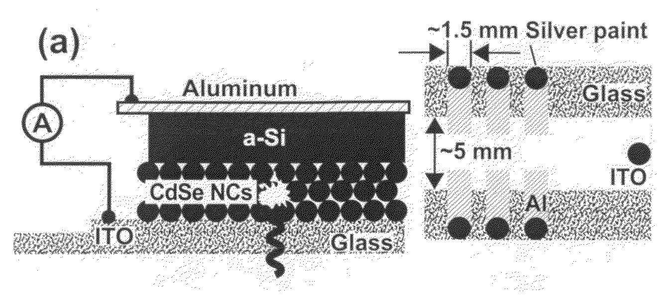
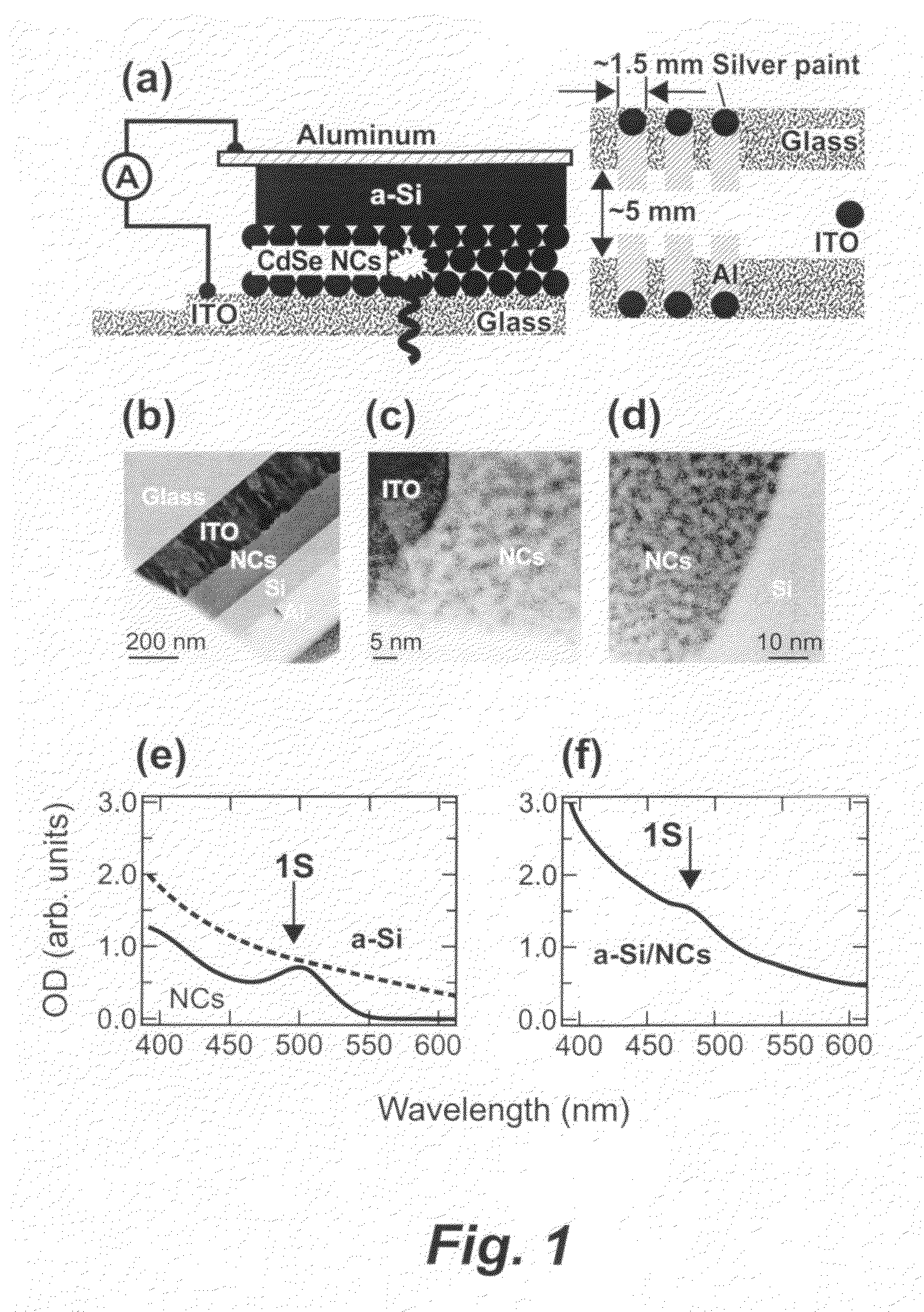
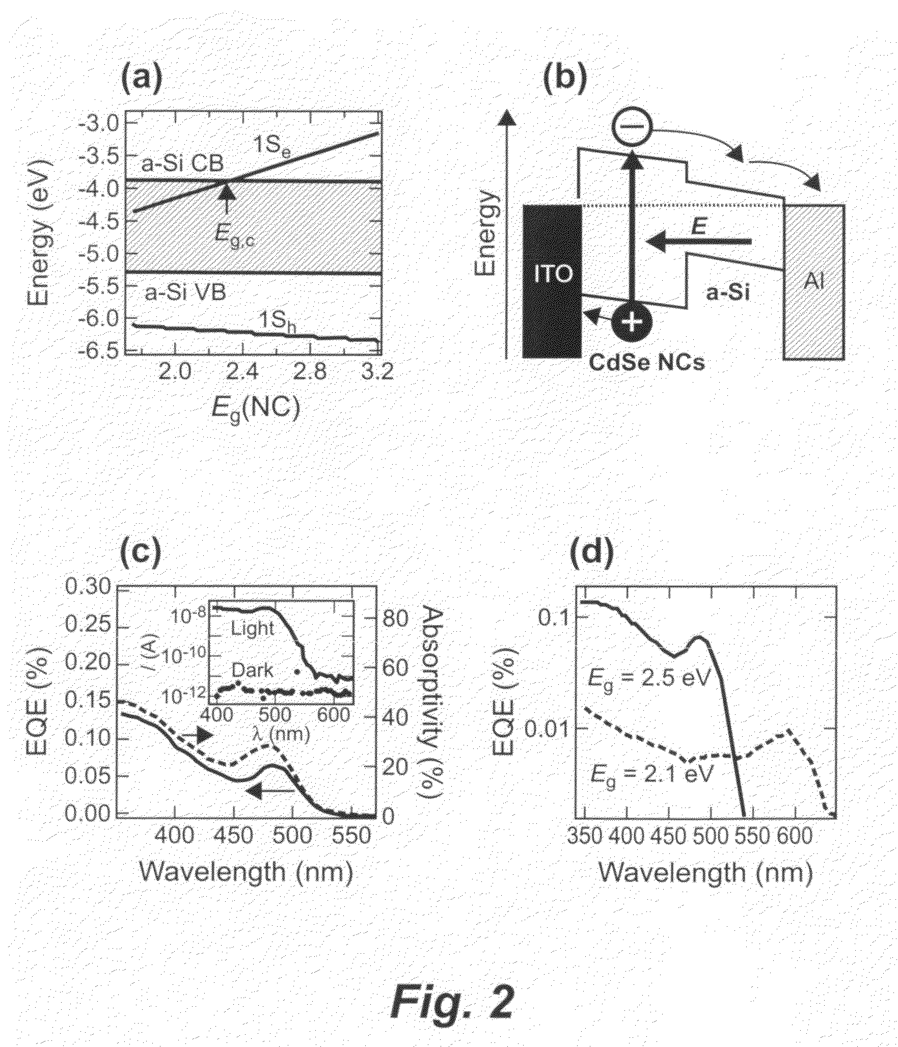
[0012]In this work, we explore a similar strategy—integration of NCs into traditional thin-film structures—but in application to PV devices. At present, the PV market is dominated by crystalline silicon (c-Si) cells. However, cost considerations have lead to rapid expansion of the PV market segment utilizing amorphous silicon (a-Si). In addition to reduced fabrication cost, a-Si provides the advantage of increased light absorptivity, which allows one to reduce the thickness of a solar cell, and hence material consumption, and the device weight. The efficiencies of a-Si solar cells are still lower than those of devices made of c-Si (˜9% versus ˜25%). Inclusion of NCs can potentially enhance the performance of a-Si PV structures through added flexibility in tailoring the device absorption spectrum, application of tandem architectures, and perhaps, increased conversion efficiency in the ultraviolet through carrier multiplication. From the fabrication prospective, integration of NCs int...


PUM


Abstract

Semiconductor nanocrystals (NCs) are promising materials for applications in photovoltaic (PV) structures that could benefit from size-controlled tunability of absorption spectra, the ease of realization of various tandem architectures, and perhaps, increased conversion efficiency in the ultraviolet through carrier multiplication. The first practical step toward utilization of the unique properties of NCs in PV technologies could be through their integration into traditional silicon-based solar cells. Here, we demonstrate an example of such hybrid PV structures that combine colloidal NCs with amorphous silicon. In these structures, NCs and silicon are electronically coupled, and the regime of this coupling can be tuned by altering the alignment of NC states with regard to silicon band edges. For example, using wide-gap CdSe NCs we demonstrate a photoresponse which is exclusively due to the NCs. On the other hand, in devices comprising narrow-gap PbS NCs, both the NCs and silicon contribute to photocurrent, which results in PV response extending from the visible to the near-infrared. This work demonstrates the feasibility of hybrid PV devices that combine advantages of mature silicon fabrication technologies with the unique electronic properties of semiconductor NCs.

Description

RELATED APPLICATIONS[0001]This application claims the priority of U.S. Provisional Patent Application 61 / 207,012, entitled “Hybrid Photovoltaics Based on Semiconductor Nanocrystals and Amorphous Silicon,” which was filed on Feb. 6, 2009, incorporated by reference herein.STATEMENT OF FEDERAL RIGHTS[0002]The United States government has rights in this invention pursuant to Contract No. DE-AC52-06NA25396 between the United States Department of Energy and Los Alamos National Security, LLC for the operation of Los Alamos National Laboratory.FIELD OF THE INVENTION[0003]The present invention relates to hybrid photovoltaic structures including both a semiconductor nanocrysal layer and a layer of an amorphous silicon.BACKGROUND OF THE INVENTION[0004]Semiconductor nanocrystals (NCs) are promising materials for the realization of low-cost, high-efficiency photovoltaics (PV). They can be synthesized and processed via solution-based techniques readily applicable to the fabrication of large-area ...

Claims


Application Information

Patent Timeline
IPC IPC(8): H01L31/00H01B1/04
CPCH01L31/03529Y02E10/50H01L31/074H01L31/03921
Inventor KLIMOV, VICTOR I.FINDIKOGLU, ALP T.SUN, BAOQUANWERDER, DONALD J.SYKORA, MILAN
Owner LOS ALAMOS NATIONAL SECURITY
Why Eureka
Try Eureka