Method of forming multi metal layers thin film on wafer

Inactive Publication Date: 2010-09-23
NAN YA TECH
View PDF3 Cites 9 Cited by
  • Summary
  • Abstract
  • Description
  • Claims
  • Application Information

AI Technical Summary

Benefits of technology

[0011]The main purpose of one of the present preferred embodiments provides a processing method for only depositing a titanium layer film on a wafer through a sputter chamber. Then, the chemical vapor deposition titanium nitride plasma is used to transform titanium into titanium nitride after physi

Problems solved by technology

Unfortunately, if capping titanium nitride by physical vapor deposition sputter process directly, particle can be a problem because of stress difference between titanium and titanium nitride.
All the procedures require considerable time and manpower.
Because of the physical vapor deposition of titanium or titanium nitride, the pa

Method used


Image

  • Method of forming multi metal layers thin film on wafer
  • Method of forming multi metal layers thin film on wafer
  • Method of forming multi metal layers thin film on wafer

Examples


Embodiment Construction

[0037]The present invention will now be described more specifically with reference to the following embodiments. It is to be noted that the following descriptions of preferred embodiments of this invention are presented herein for the purposes of illustration and description only; it is not intended to be exhaustive or to be limited to the precise form disclosed.

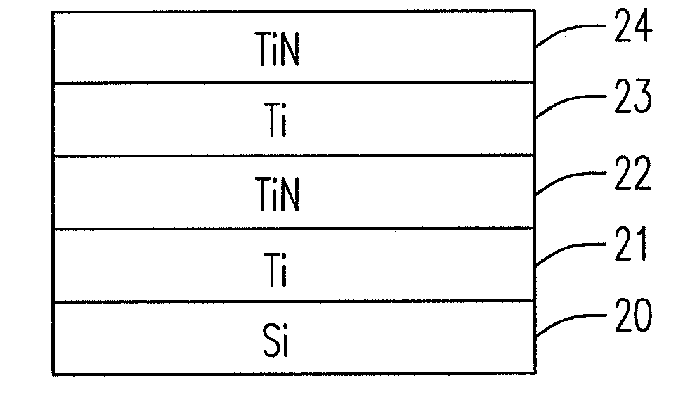
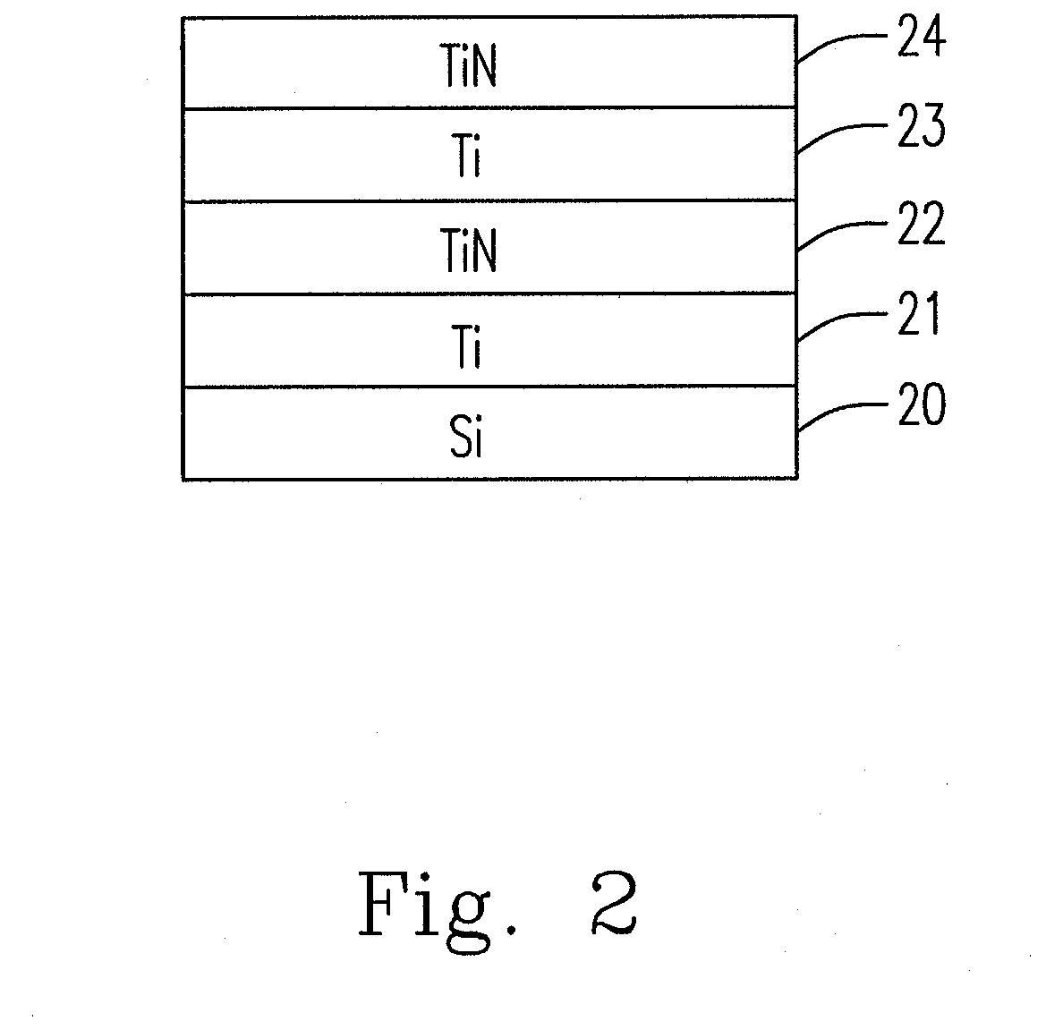
[0038]Please refer to FIG. 4, which is the profile diagram showing the present structure of the thin film deposition. The following FIGS. 4(a)˜(d) are used to illustrate the forming method for the thin film deposition of the present invention. In FIG. 4(a), a semiconductor wafer is firstly provided, wherein the semiconductor is a silicon wafer 40.

[0039]Please refer to FIG. 4(b), a titanium layer 41 is formed on the top surface of the silicon wafer 40 by physical vapor deposition sputtering method.

[0040]Please refer to FIG. 4(c), according to FIG. 4(b), a titanium nitride layer 42 is formed on the top surface of the titanium ...


PUM


Abstract

A method of forming the multi metal layers thin film has Ti sputtered on top surface of a substrate by PVD first. Then, Ti is transformed into TiN via CVD. Thus, by skipping the extra process steps of wafer cleaning and surface treating, the method not only solves the stress problems between two different metal layers but also improves the cycle time and particle performance for the production without any yield impact.

Description

FIELD OF THE INVENTION[0001]The present invention relates to a deposition process in the semiconductor field, and more particularly to a method for simplifying thin film deposition process.BACKGROUND OF THE INVENTION[0002]In the semiconductor industry, for some characteristics of the material, thin film deposition becomes one of the most popular methods to deal with the material surface. Especially, the process is used for forming a layer of homogeneous or heterogeneous material film on the surface of a wafer.[0003]A thin film on a wafer is generally manufactured through various processes, such as physical vapor deposition (PVD) or sputter deposition, chemical vapor deposition (CVD), cleaning (scrubber), anneal, as well as other specific multiple procedures to deal with the metal layer. Some chamber is usually configured as a single procedure in the overall manufacturing process, to deal with the wafer with the repeating deposition and the cleaning steps.[0004]In a typical process, ...

Claims


Application Information

Patent Timeline
IPC IPC(8): H01L21/3205C23C16/44
CPCC23C14/16C23C14/586C23C16/34H01L21/2855H01L21/76864H01L21/76846H01L21/76856H01L21/76862H01L21/28556
Inventor CHIU, YUSHANLO, YI-JEN
Owner NAN YA TECH
Why Eureka
Try Eureka