TVS with low capacitance & Forward voltage drop with depleted SCR as steering diode

a technology of forward voltage drop and tv, which is applied in the direction of diodes, circuit arrangements, semiconductor devices, etc., can solve the problems of uncontrollable high voltage accidental strike on the circuit, difficulty in controlling uniformity, etc., and achieves improved device configuration, simplified layer structure, and less area

Active Publication Date: 2010-09-30
ALPHA & OMEGA SEMICON INC
View PDF1 Cites 66 Cited by
  • Summary
  • Abstract
  • Description
  • Claims
  • Application Information

AI Technical Summary

Benefits of technology

[0011]It is therefore an aspect of the present invention to provide an improved TVS structural configurations implemented with high-side diode, low-side diode functioning as a pair of steering diodes. The steering diodes are integrated with a main Zener diode wherein the high-side diode, the low-side diode and the main Zener diode are all manufactured as vertical diodes in a semiconductor substrate with simplified layer structures. The high-side diode overlaps with the main Zener diode such that the TVS device occupies significantly less area. Meanwhile, the device configuration is improved by forming multiple PN junctions with a laterally extended N− buried layer in a P epitaxial layer below a N− to

Problems solved by technology

The device configurations and method of manufacturing the transient voltage suppression (TVS) device are still confronted with the technical challenges to further reduce the capacitance while maintaining a simplified and low cost manufacturing process and shrinking the area occupied by the TVS chips.
However, in situations such as electrostatic discharge (ESD), electrical fast transients and lightning, an

Method used


Image

  • TVS with low capacitance & Forward voltage drop with depleted SCR as steering diode
  • TVS with low capacitance & Forward voltage drop with depleted SCR as steering diode
  • TVS with low capacitance & Forward voltage drop with depleted SCR as steering diode

Examples


Embodiment Construction

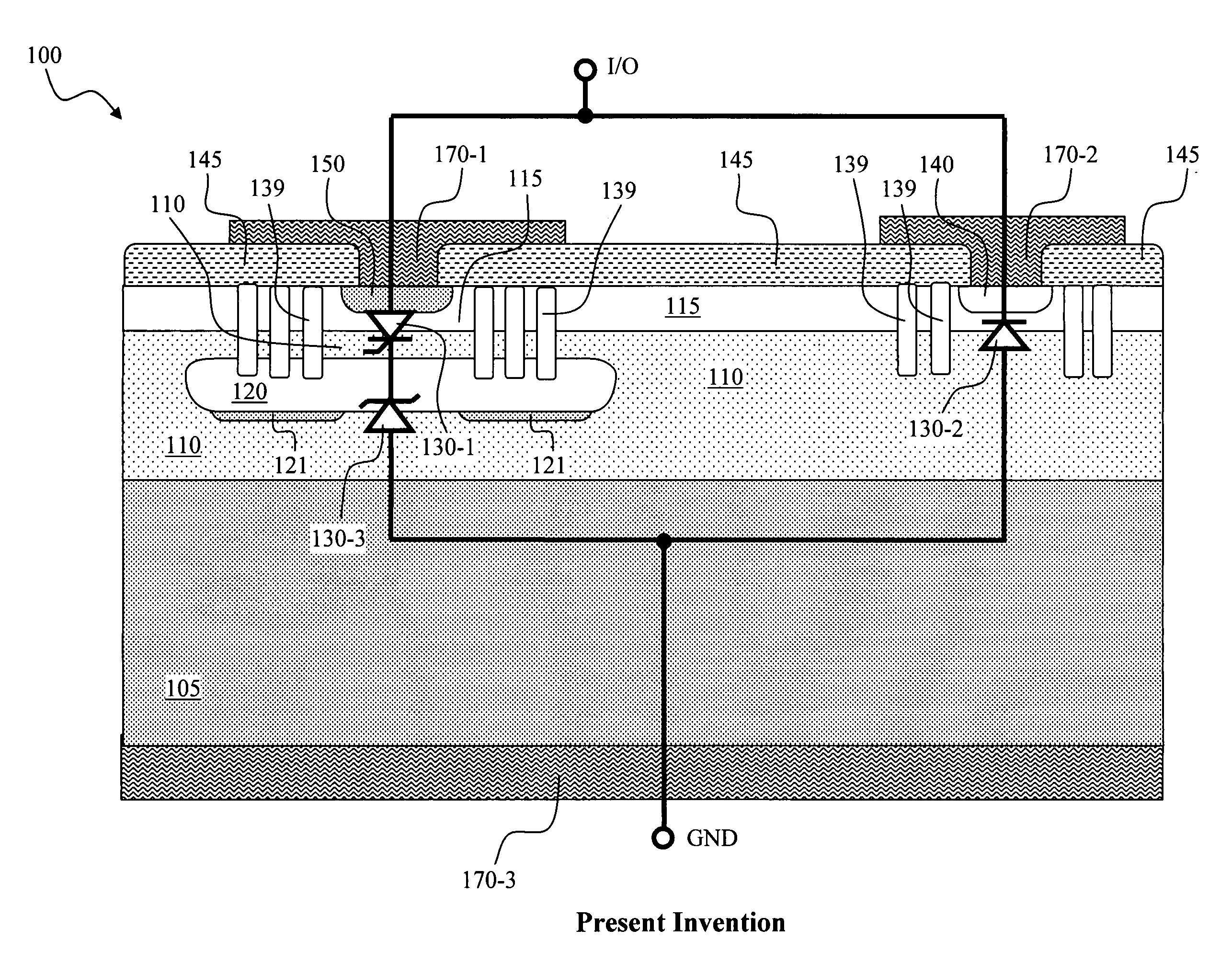
[0024]Refer to FIG. 2A for a side cross sectional view illustrated with equivalent circuit of a transient voltage suppressor (TVS) 100 of this invention. The TVS device as shown is formed with a depleted SCR high side structure using a buried N+ layer in a P type epitaxial region, with the addition of P and N type regions implanted from the top surface. The low side diode is formed by a P+ / N− / P− / N+ (or N+ / N− / P− / P+) doping profile, to achieve a lower junction capacitance. Specifically, the TVS 100 is formed on a heavily doped P+ semiconductor substrate 105 which supports a lightly doped P− epitaxial layer 110. An N− top dopant layer 115 is located at the top of P− epitaxial layer 110. The TVS 100 includes a P+ contact region 150 formed near a top surface of the semiconductor substrate, above the N buried region 120, to enhance the electrical contact with the I / O pad 170-1. The TVS 100 further includes an N+ buried region 120 formed in the P− epitaxial layer 110. A semiconductor contr...


PUM


Abstract

A transient-voltage suppressing (TVS) device disposed on a semiconductor substrate of a first conductivity type. The TVS includes a buried dopant region of a second conductivity type disposed and encompassed in an epitaxial layer of the first conductivity type wherein the buried dopant region extends laterally and has an extended bottom junction area interfacing with the underlying portion of the epitaxial layer thus constituting a Zener diode for the TVS device. The TVS device further includes a region above the buried dopant region further comprising a top dopant layer of a second conductivity type and a top contact region of a second conductivity type which act in combination with the epitaxial layer and the buried dopant region to form a plurality of interfacing PN junctions constituting a SCR acting as a steering diode to function with the Zener diode for suppressing a transient voltage.

Description

BACKGROUND OF THE INVENTION[0001]1. Field of the Invention[0002]The invention relates generally to a circuit configuration and method of manufacture of a transient voltage suppressor (TVS). More particularly, this invention relates to an improved circuit configuration and method of manufacture with simplified configuration to integrate steering diode with the Zener diode further reduce the capacitance for a transient voltage suppressor (TVS).[0003]2. Description of the Relevant Art[0004]The device configurations and method of manufacturing the transient voltage suppression (TVS) device are still confronted with the technical challenges to further reduce the capacitance while maintaining a simplified and low cost manufacturing process and shrinking the area occupied by the TVS chips. Specifically, the transient voltage suppressors (TVS) are commonly applied for protecting integrated circuits from damages due to the inadvertent occurrence of an over voltage imposed onto the integrated...

Claims


Application Information

Patent Timeline
IPC IPC(8): H01L29/866
CPCH01L27/0259H01L27/0814H01L29/866H01L29/0657H01L27/0817
Inventor BOBDE, MADHURGUAN, LINGPENGBHALLA, ANUPWENG, LIMIN
Owner ALPHA & OMEGA SEMICON INC
Why Eureka
Try Eureka