

Spin mosfet and reconfigurable logic circuit
- Summary
- Abstract
- Description
- Claims
- Application Information
AI Technical Summary
Benefits of technology
Problems solved by technology
Method used
Image

Examples
first embodiment
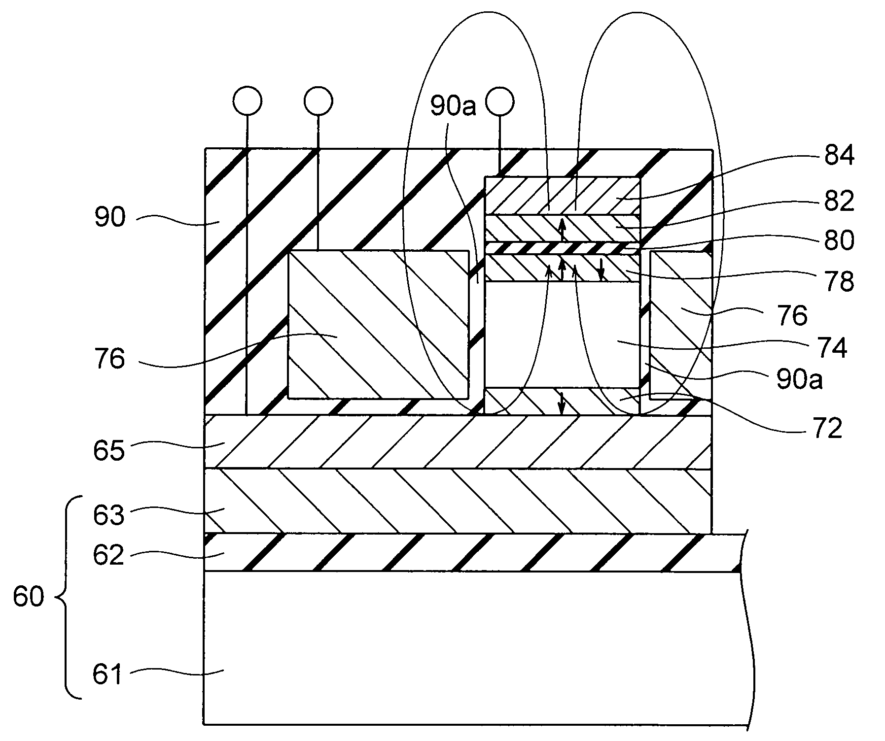
[0049]FIG. 1 shows a spin MOSFET according to a first embodiment of the present invention. The spin MOSFET of this embodiment is a vertical type spin MOSFET, and is formed on a SOI substrate 60 that includes a supporting substrate 61 made of Si, a buried oxide film 62, and a SOI (Silicon On Insulator) layer 63. The spin MOSFET may be formed on a Si bulk substrate, instead of a SOI substrate. A base layer 65 is formed on the SOI layer 63. A ferromagnetic layer 72 that has magnetization substantially perpendicular to a film plane and has a fixed magnetization direction is formed on the base layer 65. In this specification, a “film plane” of a ferromagnetic layer is an upper face of the ferromagnetic layer. A channel layer 74 that is formed from p-type semiconductor crystals is formed on the ferromagnetic layer 72. A free layer 78 that has a variable magnetization direction and is formed of a ferromagnetic layer is formed on the channel layer 74. A tunnel barrier 80 is formed on the fr...
second embodiment
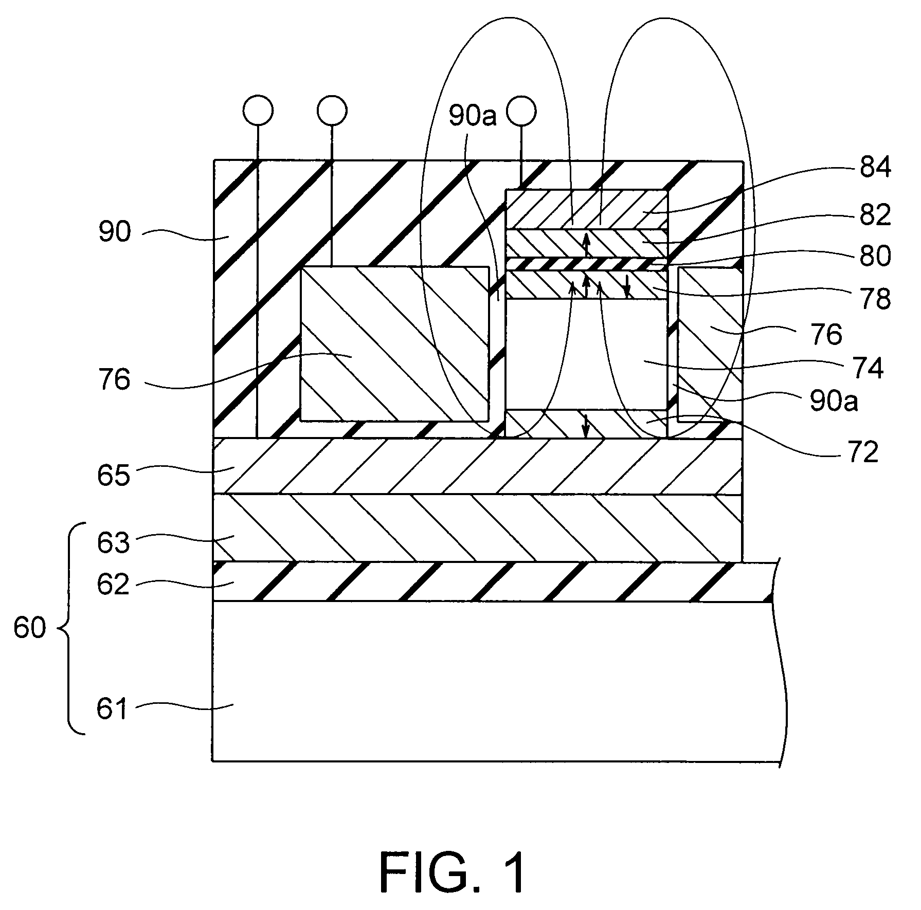
[0056]FIG. 2 is a spin MOSFET according to a second embodiment of the present invention. The spin MOSFET of this embodiment is a vertical spin MOSFET, and is the same as the spin MOSFET of the first embodiment shown in FIG. 1, except that a tunnel barrier 73 is provided between the channel layer 74 formed from semiconductor crystals and the ferromagnetic layer 72, and a tunnel barrier 77 provided between the channel layer 74 and the free layer 78. If tunnel barriers made of a material such as MgO that can epitaxially grow even if the channel layer 74 is made of Ge or GaAs are used as the tunnel barriers 73 and 77, the tunnel barriers 73 and 77 can also serve as diffusion barriers, and advantageously improve the resistance to device pressure. In this embodiment, a stacked structure that is formed of the ferromagnetic layer 72, the tunnel barrier 73, the channel layer 74 formed from semiconductor crystals, the tunnel barrier 77, the free layer 78, the tunnel barrier 80, the ferromagne...
third embodiment
[0059]FIG. 3 is a cross-sectional view of a spin MOSFET according to a third embodiment of the present invention. The spin MOSFET of this embodiment is a lateral n-type spin MOSFET that is formed in a device region 3 of a p-type semiconductor substrate 2. This device region 3 is a semiconductor region divided by device-insolating insulating films 4. The semiconductor region may be part of a semiconductor substrate, or may be a well region formed on a semiconductor substrate. Alternatively, the semiconductor region may be a SOI layer on a SOI substrate. In this specification, the device region 3 may be a semiconductor region that is part of a p-type semiconductor substrate, or may be a p-well region formed on an n-type substrate. In this device region 3, an n-type impurity diffusion region 6a and an n-type impurity diffusion region 6b are formed at a distance from each other. An n+-impurity diffusion region 7a and an n+-type impurity diffusion region 7b having higher density than the...
PUM
 Abstract
Description
Claims
Application Information