Solid-state imaging device, driving method of solid-state imaging device, and electronic apparatus

a technology of solid-state imaging and driving method, which is applied in the direction of color television, television system scanning details, and system scanning details, etc., can solve the problems of affecting the withstand voltage consideration of solid-state imaging devices, and the mounting of such elements becomes difficult in view of a manufacturing process, so as to reduce the number of connection terminals and reduce the blur effect of pixel blurring

Active Publication Date: 2010-09-30
SONY CORP
View PDF9 Cites 151 Cited by
  • Summary
  • Abstract
  • Description
  • Claims
  • Application Information

AI Technical Summary

Benefits of technology

[0043]Since the delay and the waveform deformation in the drive pulse driving the pixel are controlled, a high-speed operation having concurrency in the driving of the pixels is performed, and pixel blurring is reduced.
[0044]Since the electrical connection between the first and second chips has a three-dimensional structure, the limitation to the number of connection terminals is eliminated. The multi-point tuning correction oper

Problems solved by technology

The technique of the related art disclosed in Japanese Unexamined Patent Application Publication No. 2007-208926 is based on a limited amount of information related to fault information and characteristic information of the solid-state imaging device.
To write information, however, the non-volatile memory typically operates from a voltage as high as 10 to 20 V. On the other hand, the solid-state imaging device typical

Method used


Image

  • Solid-state imaging device, driving method of solid-state imaging device, and electronic apparatus
  • Solid-state imaging device, driving method of solid-state imaging device, and electronic apparatus
  • Solid-state imaging device, driving method of solid-state imaging device, and electronic apparatus

Examples


first embodiment

1. First Embodiment

1.1 Structure of Solid-State Imaging Device

[0073]FIG. 3A is a perspective view diagrammatically illustrating a solid-state imaging device 1 of a first embodiment of the present invention, and FIG. 3B is a block diagram illustrating the solid-state imaging device 1 of the first embodiment of the present invention.

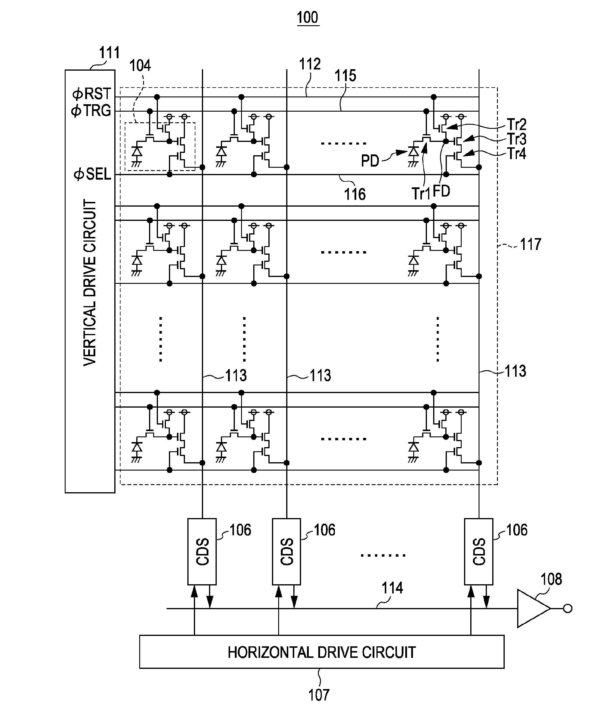
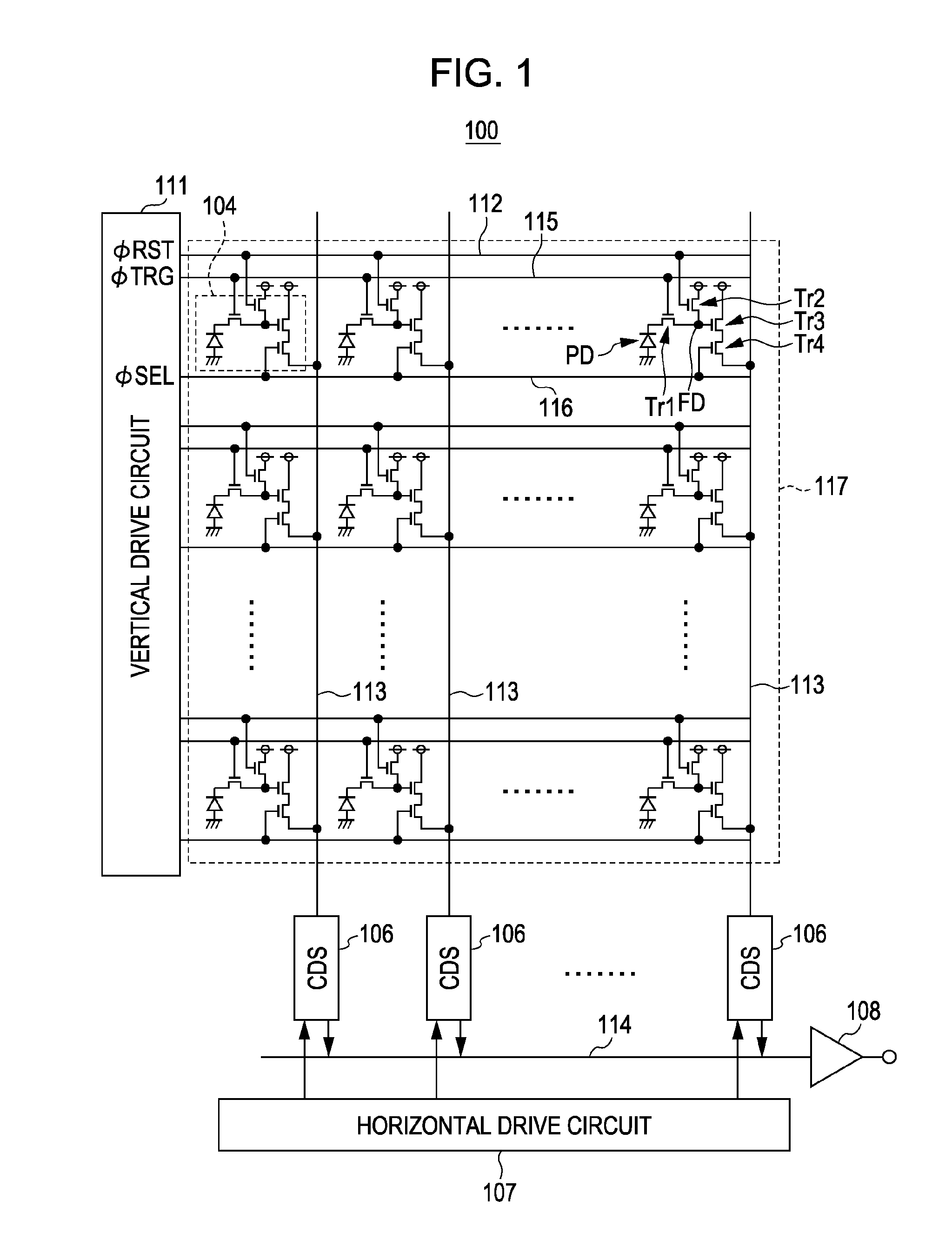
[0074]The solid-state imaging device 1 includes first chip 2, second chip 3, pixels 4, pixel module 5, column signal processing circuits 6, horizontal drive circuit 7, output circuit 8, control circuit 9, timing synchronization circuit 10, pixel drive circuit 11, connection units 12, vertical signal lines 13, horizontal signal line 14, and substrate 15. The pixel 4 includes light sensing unit 16, floating diffusion unit 17, a charge storage capacitance 17a, a floating diffusion region 17b, impurity regions 18, 19, and 20, gate electrodes 21, 21a, 21b, 22, 22a, 22b, 23, and 24, gate insulator 25, a plurality of wiring layers 26, interlayer insulator 27, wir...

second embodiment

2. Second Embodiment

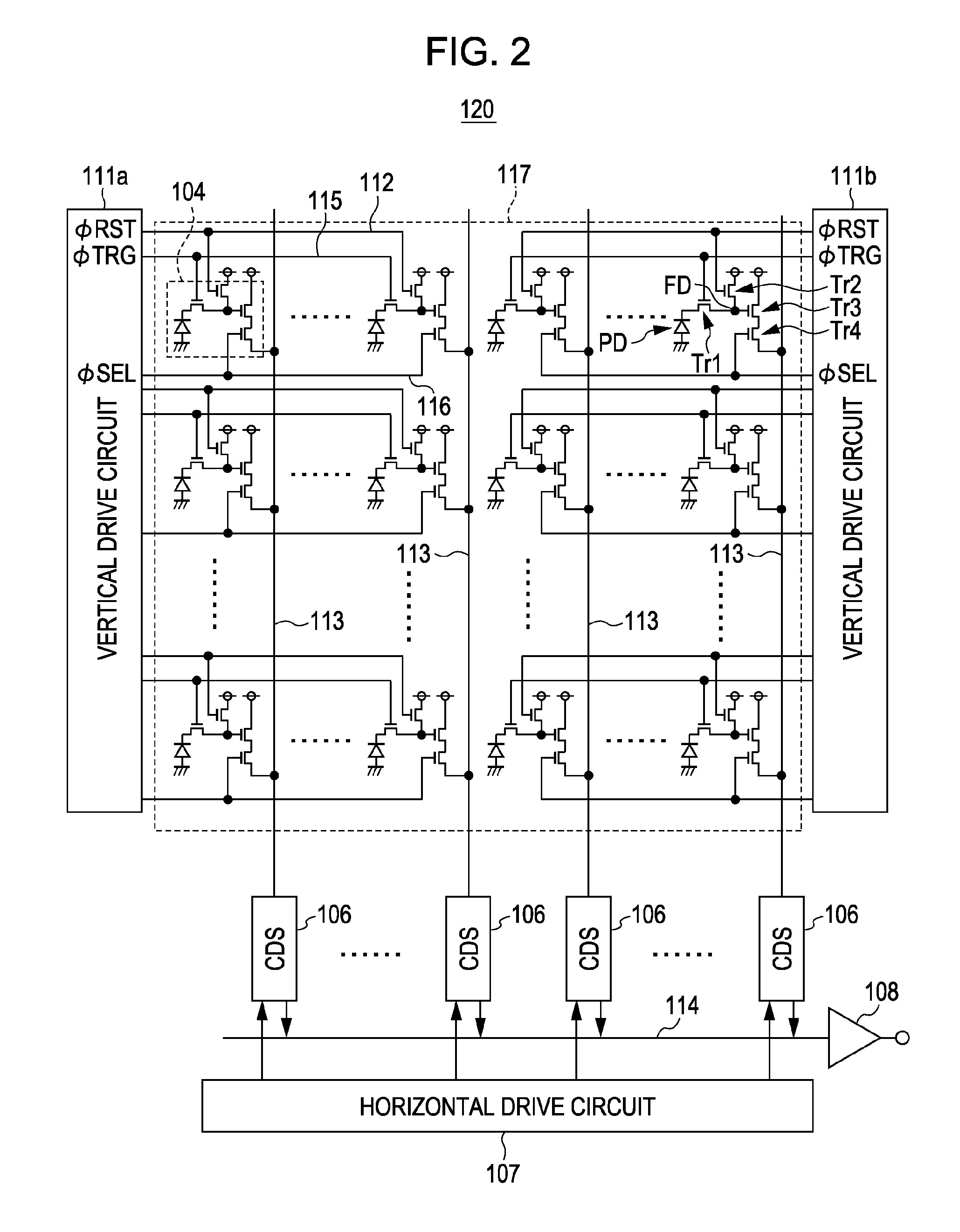
[0135]A solid-state imaging device of a second embodiment of the present invention is described below. FIG. 10A is a perspective view diagrammatically illustrating a solid-state imaging device 41 in accordance with the second embodiment of the present invention, and FIG. 10B is a top view diagrammatically illustrating the solid-state imaging device 41 in accordance with the second embodiment. FIG. 11A is a block diagram diagrammatically illustrating a first chip 42, and FIG. 11B is a block diagram diagrammatically illustrating a second chip 43.

[0136]In FIGS. 10A and 10B, and 11A and 11B, elements identical those illustrated in FIGS. 3A and 3B and 4A and 4B are designated with the same reference numerals and the discussion thereof is omitted herein.

[0137]The second chip 43 of the second embodiment includes control circuit 9, timing synchronization circuit 10, and pixel drive circuit 40. The second chip 43 also includes the column signal processing circuit 6, the h...

third embodiment

3. Third Embodiment

[0147]A solid-state imaging device of a third embodiment of the present invention is described below. FIG. 13 is a sectional view diagrammatically illustrating a pixel, a pixel drive circuit, and a connection unit in the solid-state imaging device of the third embodiment of the present invention. The solid-state imaging device of the third embodiment remains unchanged in general structure from the solid-state imaging device 1 illustrated in FIGS. 3A and 3B, and the discussion thereof is omitted here. In FIG. 13, elements identical to those illustrated in FIG. 5 are designated with the same reference numerals and the discussion thereof is omitted here.

[0148]The solid-state imaging device of the third embodiment is of a top light incident type. A first chip 63 is different in structure to the counterpart in the first embodiment.

[0149]As illustrated in FIG. 13, the first chip 63 includes substrate 55 having the light sensing unit 56, a plurality of wiring layers 61, ...


PUM


Abstract

A solid-state imaging device includes a first chip including a plurality of pixels, each pixel including a light sensing unit generating a signal charge responsive to an amount of received light, and a plurality of MOS transistors reading the signal charge generated by the light sensing unit and outputting the read signal charge as a pixel signal, a second chip including a plurality of pixel drive circuits supplying desired drive pulses to pixels, the second chip being laminated beneath the first chip in a manner such that the pixel drive circuits are arranged beneath the pixels formed in the first chip to drive the pixels, and a connection unit for electrically connecting the pixels to the pixel drive circuits arranged beneath the pixels.

Description

BACKGROUND OF THE INVENTION[0001]1. Field of the Invention[0002]The present invention relates to solid-state imaging devices, and in particular to a CMOS type solid-state imaging device and a drive method of the solid-state imaging device. The present invention also relates to an electronic apparatus including the solid-state imaging device.[0003]2. Description of the Related Art[0004]Video cameras and digital still cameras are in widespread use. Such a camera includes a charge-coupled device (CCD) solid-state imaging device or an amplified solid-state imaging sensor. The amplified solid-state imaging device guides a signal charge, generated and stored at a light sensing unit of each pixel, to an amplifier, and then outputs a signal, amplified by the amplifier in response to the signal charge, from the pixel. A plurality of such pixels are arranged in a matrix. The amplified solid-state imaging devices also include a solid-state imaging device having junction-type field effect trans...

Claims


Application Information

Patent Timeline
IPC IPC(8): H04N5/335H04N5/374H04N5/376
CPCH01L27/14627H01L27/14634H01L27/14636H04N5/2257H01L27/1464H04N5/374H04N5/3765H04N5/363H04N5/335H04N23/57H04N25/00H04N25/745H04N25/79H04N25/76H04N25/65
Inventor HONDA, KATSUMITAKATSUKA, TAKAFUMI
Owner SONY CORP
Why Eureka
Try Eureka