Organic el device, method of manufacturing organic el device, and electronic device

a manufacturing method and organic el technology, applied in the manufacture of electrode systems, electric discharge tubes/lamps, discharge tubes luminescent screens, etc., can solve the problems of poor connection, degraded luminance of organic el devices, etc., and achieve high color purity

Active Publication Date: 2010-10-07
ELEMENT CAPITAL COMMERCIAL CO PTE LTD
View PDF0 Cites 47 Cited by
  • Summary
  • Abstract
  • Description
  • Claims
  • Application Information

AI Technical Summary

Benefits of technology

[0010]According to such a configuration, the anti-reflection layer is provided on the reflection layer in an area except for the first area, where the optical resonator has a resonance wavelength corresponding to a color of the light emitted from the pixels, out of the area of the pixels. In an area where the anti-reflection layer is provided on the reflection layer, since reflection of the light is suppressed, the light from the organic functional layer hardly resonates between the reflection layer and the second electrode in the area except for the first area. For this reason, it is possible to suppress degradation of the luminance caused when light beams having different resonance wavelengths are mixed in the area of the pixels. As a result, it is possible to provide an organic EL device having a higher luminance.Application 2
[0016]According to such a configuration, it is possible to conductively connect the first electrode and the driving element with the reflection layer. Consequently, it is possible to improve freedom in selecting an arrangement position of the driving element in a design stage of the organic EL device.Application 5
[0024]According to such a method, it is possible to the adjust resonance wavelength of the optical resonator depending on the color of the light emitted from the pixel using the layer thickness of the first electrode. Since the first electrode is formed with the same layer thickness in at least the first area, when a portion where the layer thickness of the first electrode is different exists, that portion is arranged in the area where the anti-reflection layer is provided. Since the reflection of light is suppressed in the area where the anti-reflection layer is provided on the inflection layer, the light from the organic functional layer hardly resonates between the reflection layer and the second electrode in an area except for the first area. For this reason, it is possible to suppress degradation of the luminance caused by mixing the light beams having different resonance wavelengths in the area of pixels. As a result, it is possible to manufacture an organic EL device having a higher luminance.Application 9

Problems solved by technology

In addition, since the reflection layer and the insulation film are arranged in three-layers between the positive electrode and the circuit portion, the contact hole may be lengthened so that risks such as bad connection may increase.
As a result, the luminance of the organic EL device may be degraded.

Method used


Image

  • Organic el device, method of manufacturing organic el device, and electronic device
  • Organic el device, method of manufacturing organic el device, and electronic device
  • Organic el device, method of manufacturing organic el device, and electronic device

Examples


first embodiment

Organic EL Device

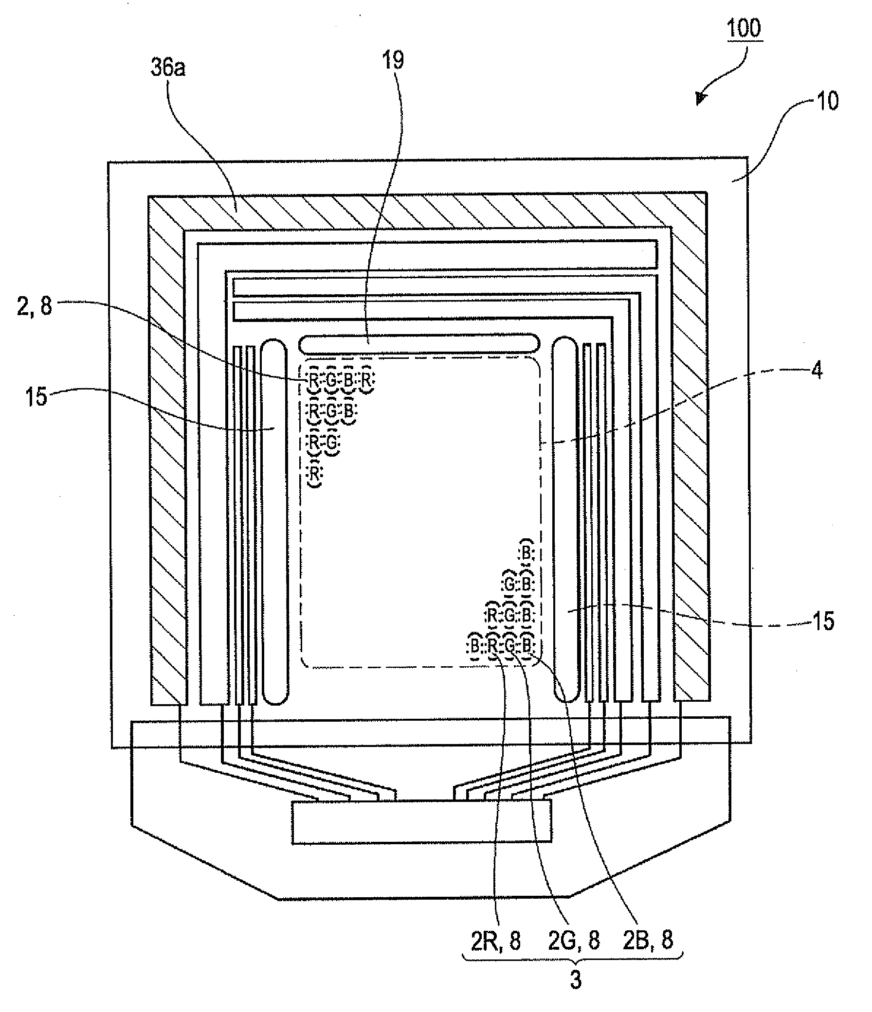
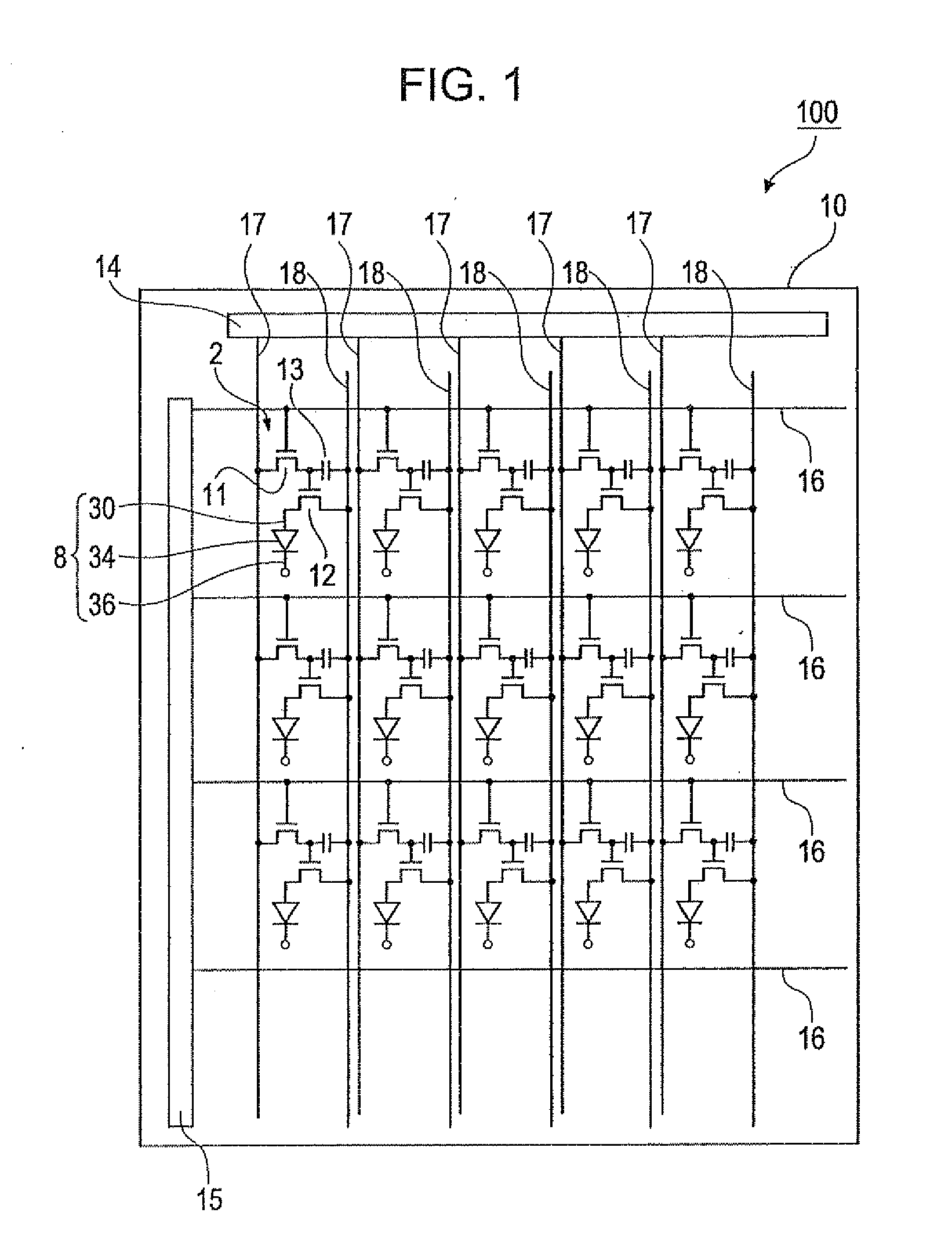
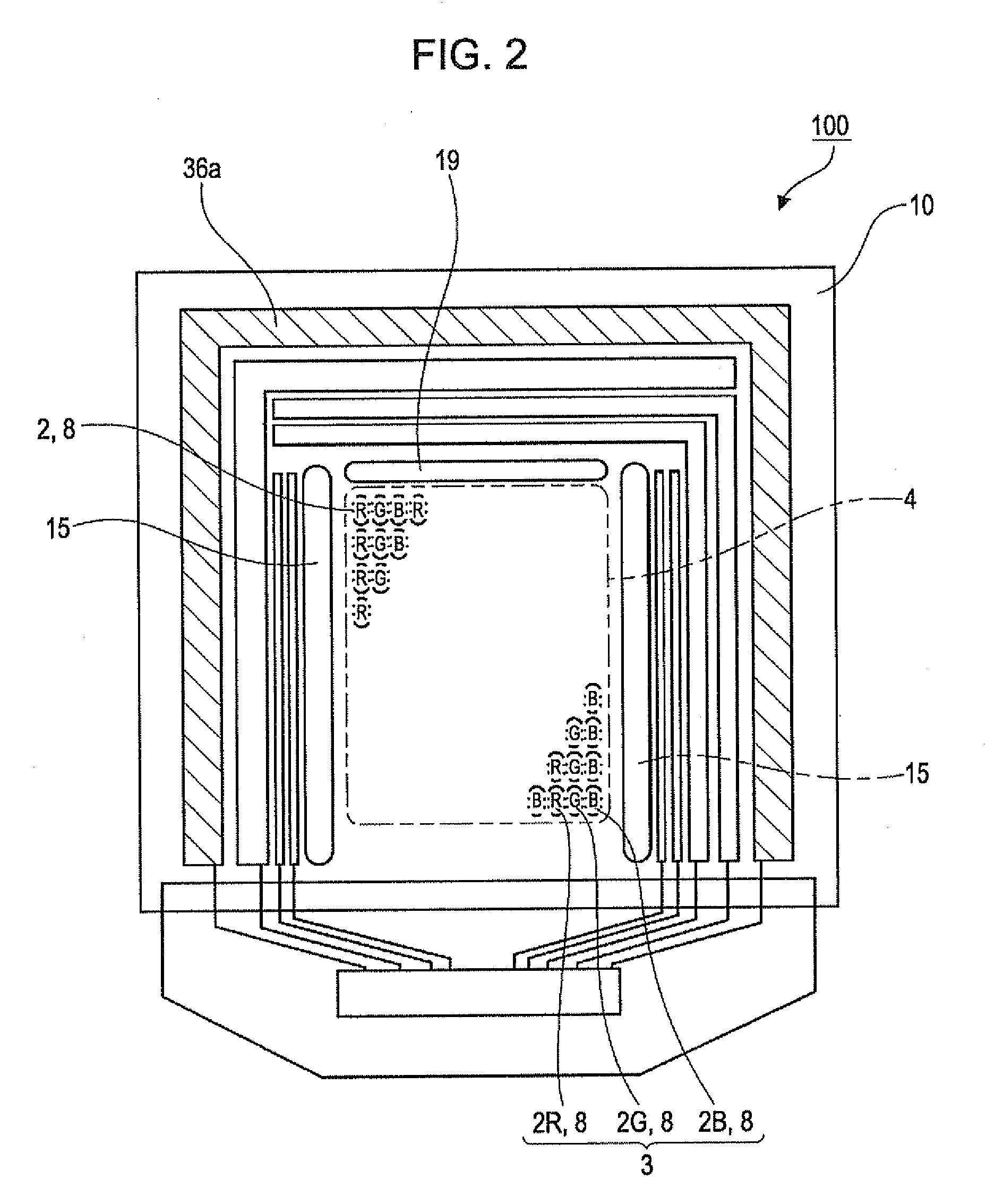
[0049]First, a configuration of an organic EL device according to first embodiment of the invention will be described with reference to the accompanying drawings. FIG. 1 is a block diagram illustrating an electric configuration of the organic EL device according to a first embodiment of the invention. FIG. 2 is a plan view schematically illustrating an organic EL device according to a first embodiment of the invention. FIG. 3 is a plan view illustrating a configuration of pixels of an organic EL device according to a first embodiment of the invention. Specifically, FIGS. 2 and 3 are plan views as seen from the color filter 40 side shown in FIG. 4. In FIG. 3, the organic functional layer 34, the negative electrode 36, the encapsulation layer 38, and the color filter 40 are omitted. FIGS. 4 and 5 are cross-sectional views schematically illustrating an organic EL device according to a first embodiment of the invention. Specifically, FIG. 4 is a cross-sectional view alo...

second embodiment

Organic EL Device

[0129]Next, the configuration of the organic EL device according to a second embodiment of the invention will be described with reference to the accompanying drawings. FIG. 11 is a plan view representing a configuration of the pixel of the organic EL device according to a second embodiment of the invention. FIG. 12 is a cross-sectional view schematically illustrating a configuration of the organic EL device according to a second embodiment of the invention. Specifically, FIG. 12 is a cross-sectional view along the line D-D of FIG. 11. In addition, since the cross-sectional view along the line A-A of FIG. 11 is commonly used in the first embodiment of the invention, a description thereof will be omitted.

[0130]The organic EL device 200 according to a second embodiment of the invention is different from the organic EL device 100 according a first embodiment of the invention in the configuration of the positive electrode 30, and other elements are similar. Like referenc...

modified example 1

[0142]While, in the organic EL device of the aforementioned embodiments, the reflection layer is provided in each pixel, the present invention is not limited thereto. Instead, the reflection layer may be provided commonly between a plurality of pixels in the organic EL device.

[0143]FIG. 14 is a plan view illustrating a configuration of the pixel in the organic EL device according to a modified example 1 of the invention. The organic EL device 300 according to a modified example 1 is different from the organic EL device 100 according to the first embodiment in the configurations of the reflection layer and the anti-reflection layer, but other elements are similar. Like reference numerals denote like elements as in the first embodiment, and descriptions thereof will be omitted.

[0144]Referring to FIG. 14, the organic EL device 300 according to a modified example 1 of the invention includes a first reflection layer 42 and a second reflection layer 46 instead of the reflection layer 24 o...


PUM


Abstract

An organic EL device includes: a base body; pixels that are arranged in the base body and emit light beams having either of at least two different colors from among red, green and blue; an reflection layer that has optical reflectivity and arranged on the base body; an anti-reflection layer that is arranged on the reflection layer and has optical reflectivity lower than that of the reflection layer; an insulation layer that is arranged on the anti-reflection layer and has optical transmittance; a first electrode that is arranged in each pixel on the insulation layer and has optical transmittance; an organic functional layer that is arranged on the first electrode and includes at least a luminescent layer; a second electrode that is arranged on the organic functional layer and has optical reflectivity and optical transmittance; and an optical resonator that is formed between the reflection layer and the second electrode to resonate the light from the organic functional layer, wherein the optical resonator has a resonance wavelength corresponding to the color of the light emitted from the pixels in a first area out of an area of the pixels, and the anti-reflection layer is provided in an area except for the first area out of the area of the pixels.

Description

BACKGROUND[0001]1. Technical Field[0002]The present invention relates to an organic EL device, a method of manufacturing an organic EL device, and an electronic device.[0003]2. Related Art[0004]The organic electroluminescence device (hereinafter, referred to as an organic EL device) includes a stack of a positive electrode, an organic functional layer having at least a luminescent layer, and a negative electrode. For example, a top-emission type organic EL device is provided with a positive electrode or a reflection layer having optical reflectivity, so that the light generated from the luminescent layer is emitted to the negative electrode side.[0005]In order to increase the luminance of the light emitted from the organic EL device, a method of amplifying and extracting the light having a resonance wavelength using an optical resonator for resonating the light from an organic functional layer included between a negative electrode and a reflection layer provided under a positive ele...

Claims


Application Information

Patent Timeline
Patent Type & Authority Applications(United States)
IPC IPC(8): H01J7/44H01L51/54H01J9/02
CPCH01L27/3248H01L51/5206H01L2251/558H01L51/5271H01L51/5265H10K59/352H10K59/121H10K59/123H10K50/813H10K50/816H10K50/852H10K50/856H10K2102/351
Inventor KOSHIHARA, TAKESHI
Owner ELEMENT CAPITAL COMMERCIAL CO PTE LTD
Why Eureka
Try Eureka