Substrate cleaning method for removing oxide film

a cleaning method and oxide film technology, applied in semiconductor devices, electric discharge tubes, chemical instruments and processes, etc., can solve the problems of large apparatus, inability to completely remove watermarks, and inability to control the etching of very thin oxide films, so as to reduce native oxide films and organic impurities, and improve the flatness of substrate surfaces. , the effect of reducing the flatness

Inactive Publication Date: 2010-10-07
CANON ANELVA CORP
View PDF20 Cites 48 Cited by
  • Summary
  • Abstract
  • Description
  • Claims
  • Application Information

AI Technical Summary

Benefits of technology

[0034]The present invention performs substrate treatment which can decrease the native oxide film and organic impurities on the surface of semiconductor substrate compared with the wet-cleaning in the related art, and can remove the native oxide film and organic matter without deteriorating the flatness of the substrate surface.
[0035]According to the present invention, to remove the native oxide film and contamination of organic impurities from the surface of semiconductor substrate, HF gas or a mixed gas containing at least HF is used as the plasma-forming gas and the treatment gas, and radicals are fed from the plasma-forming chamber to the treatment chamber, while feeding simultaneously gas molecules containing HF as the structural element thereto, thus exposing the surface of semiconductor substrate to the above atmosphere which suppresses the excitation energy of the radicals, to thereby remove the native oxide film and organic matter without deteriorating the flatness of the substrate surface. There generates no metal contamination and plasma damage on the semiconductor substrate. Although the wet-cleaning in the related art needs more than one step for the substrate treatment applying also succeeding steps such as annealing treatment, the present invention performs the substrate treatment in only one step, which attains desired effect efficiently, reduces cost, and significantly improves the treatment speed. Furthermore, use of a shower plate to the plasma-forming gas allows uniform feeding of the product gas, use of through-holes on the electrode part allows discharge even at a low power, and use of a plasma-confinement electrode plate for plasma separation provided with a plurality of radical-passing holes allows radicals in the produced plasma to be fed uniformly to the treatment chamber. By using HF as the plasma-forming gas, feeding the radicals from the plasma-forming chamber to the treatment chamber, and simultaneously feeding HF to the treatment chamber, the surface treatment provided fine surface roughness at an order of atomic layer thickness, which then realized to form a single crystal Si and SiGe film on the surface.
[0036]By the first step of conducting substrate surface treatment, and the second step of transferring the substrate without exposing the single crystal film to atmospheric air, the amount of impurities at the interface is smaller than that appears in the atmospheric transfer, and thus good device characteristics are attained.
[0037]By conducting the first step of conducting substrate surface treatment, the second step of forming single crystal film, the third step of sputtering the dielectric material to form a film, the fourth step of conducting oxidation, nitrification, or oxynitrification, and the fifth step of transferring the metallic material and the sputtered film in a vacuum without exposing thereof to atmospheric air, the amount of impurities on the joint interface between the semiconductor and the insulation film becomes smaller than that in atmospheric transfer, which provides the interface state density and the fixed charge density in film equivalent to those of oxide film attained in the related art, gives a C-V curve with small hysteresis, gives a small leak current, and thereby attains good device characteristics.

Problems solved by technology

The wet-cleaning has, however, problems of failing to completely remove water-marks in dry state, failing to control etching of very thin oxide film, requiring large apparatus, and the like.
Furthermore, when the semiconductor substrate is exposed to atmospheric air for a long time after the wet-cleaning, there arise problems of forming native oxide film on the surface thereof and adsorbing carbon atoms thereon to inhibit film-forming of Si single crystal, generating irregular profile of film, generating impurity level at the interface of gate insulation film, and the like.
However, as miniaturization of device progresses and dielectric insulation film / metal electrode is used, the device needs to be manufactured at lower temperatures.
In that case, problems arise such that oxide film is immediately formed on the Si-absent portion, that contaminants likely adhere to the dangling bond of Si, and that the sputtered oxide and contaminants adhere again to the side wall of the substrate.
These problems adversely affect the succeeding step, (such as inhibition of epitaxial growth and formation of highly resistant portion on the silicide interface).
Furthermore, damages on the device are also the problem.
There arises a problem of generating irregular surface on removing the silicon oxide film from the substrate surface.
In that case, there arise problems that the oxide film is immediately formed on the Si-absent portion, that the contaminants likely adhere to the dangling bond of Si, and that the sputtered oxide and contaminants adhere again to the side wall of the substrate.
These problems adversely affect the succeeding stage, (such as inhibition of epitaxial growth and formation of highly resistant portion on the silicide interface).
Furthermore, damages on device are also the problem.
When fluorine residue on the surface of the substrate is removed by the hydrogen radicals and the hydrogen ions, there arise problems of contamination by metal coming from the chamber, of excess etching because of large etching rate on the base Si, and the like.
Furthermore, since HF as the reaction product likely adheres again to the surface of the substrate, sufficient F-removal effect is not attained.
Since, however, the surface of the semiconductor substrate cannot be exposed to an atmosphere which suppresses the excitation energy of radicals, etching with high Si selectivity cannot be conducted, which then raises a problem of failing to remove the native oxide film without deteriorating the surface roughness.
The removal, however, did not satisfy the flatness required in recent years.

Method used


Image

  • Substrate cleaning method for removing oxide film
  • Substrate cleaning method for removing oxide film
  • Substrate cleaning method for removing oxide film

Examples


Embodiment Construction

[0069]Examples of the present invention will be described below.

[0070]Embodiments of the present invention will be described below referring to the drawings.

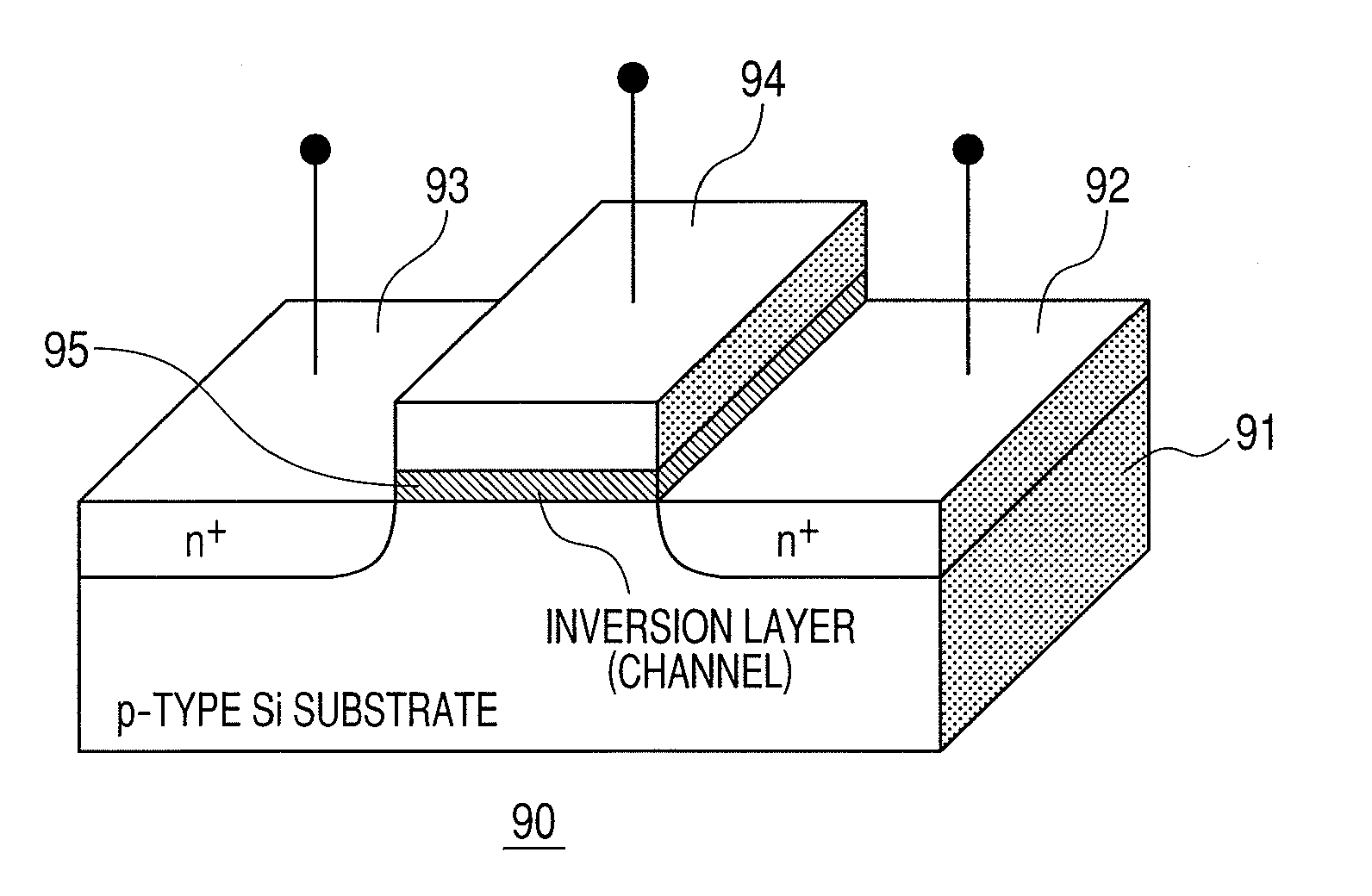
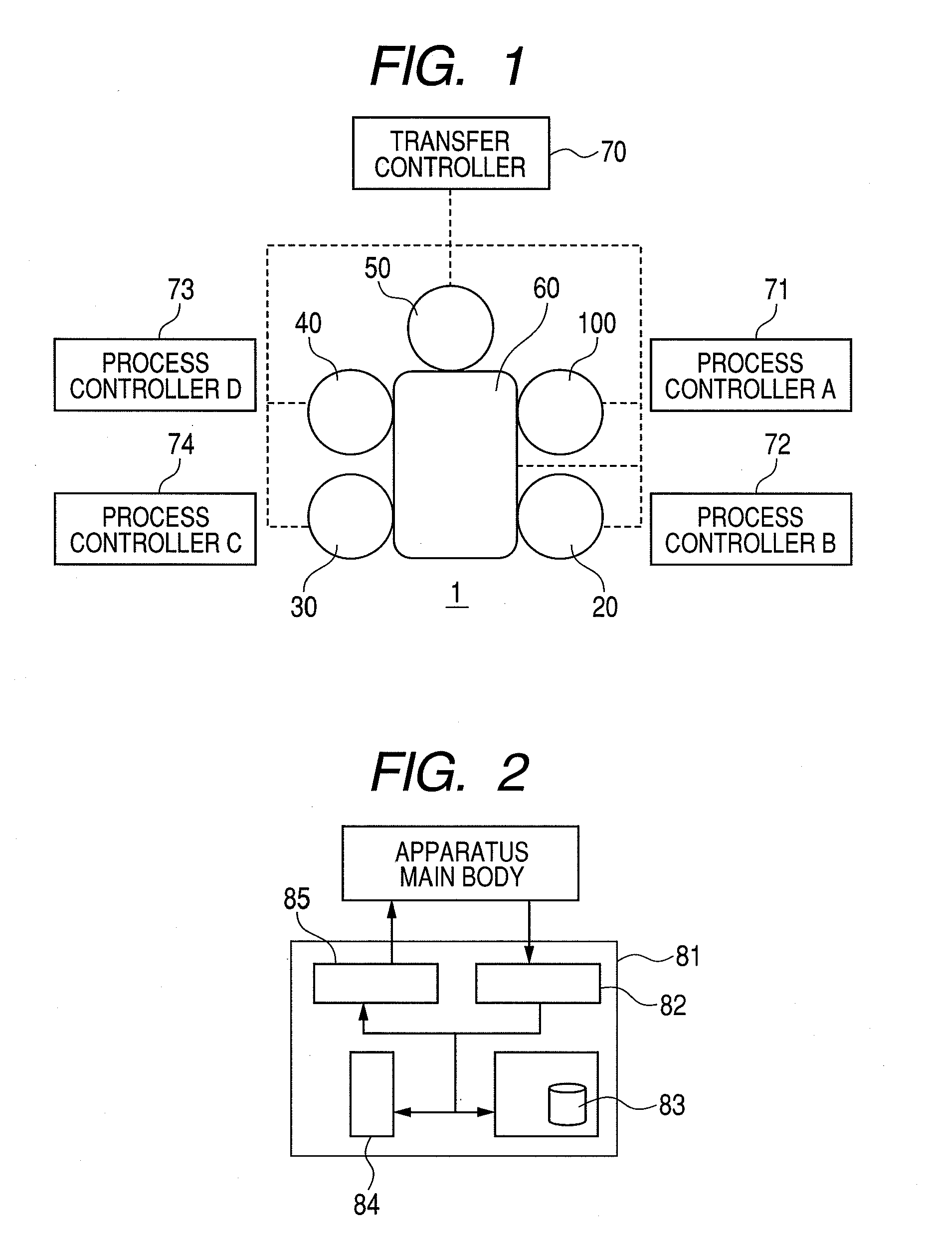
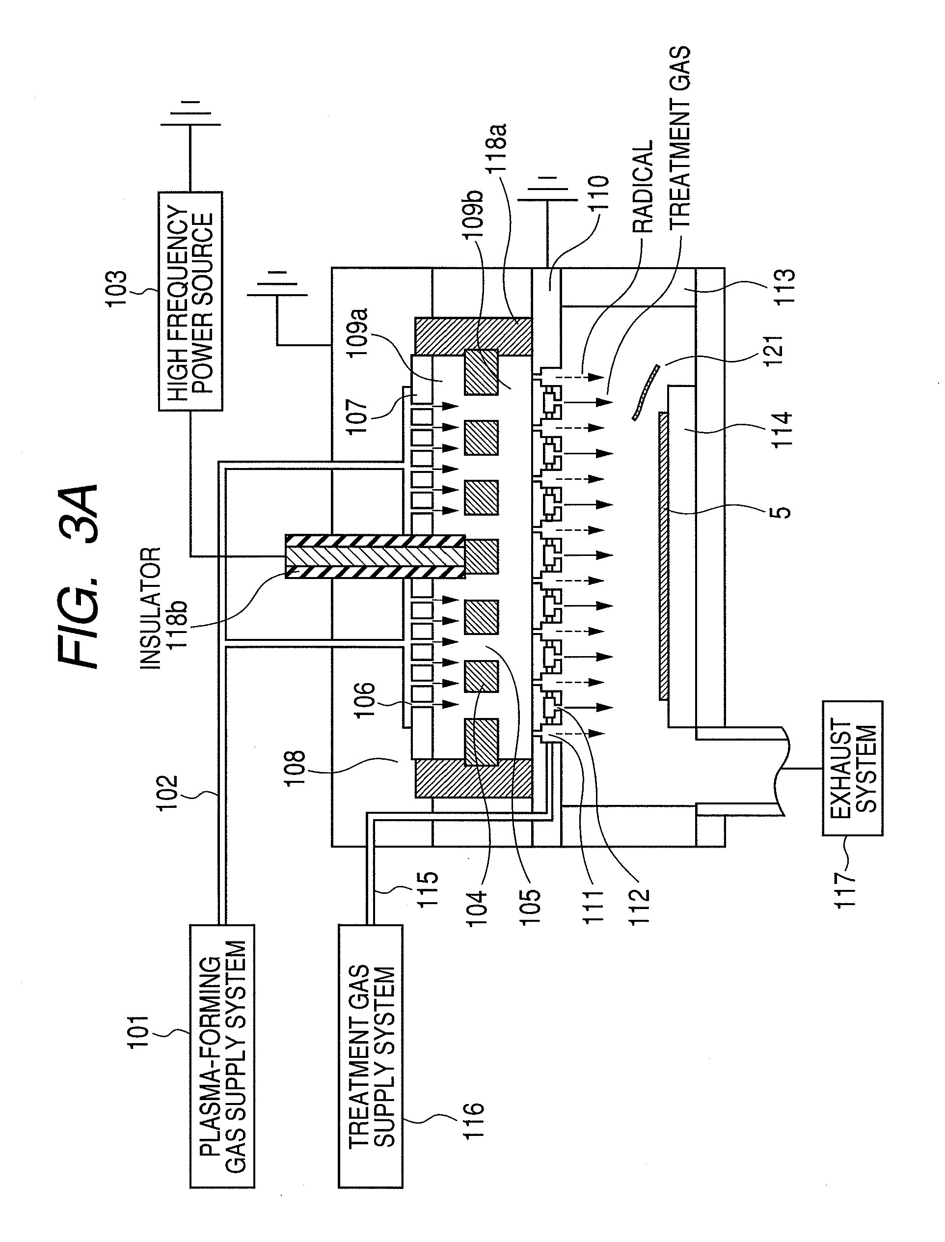
[0071]The examples deal with the cases of applying the present invention to a film-forming apparatus 1 illustrated in FIG. 1, focusing on a process of removing a native oxide film and organic matter formed on a Si substrate by the first step using a surface treatment apparatus 100 illustrated in FIGS. 3A to 3D.

[0072]A substrate 5 adopted as the sample is a Si single crystal substrate (with 300 mm in diameter) which is allowed to stand in a clean air to form a native oxide film thereon. The substrate 5 is transferred to a load-lock chamber 50 by a substrate-transfer mechanism (not shown), and is placed therein. Then, the load-lock chamber 50 is evacuated by an evacuation system (not shown). After evacuating to a desired pressure, or 1 Pa or below, a gate valve (not shown) between the load-lock chamber and a transfer chamber is op...


PUM

PropertyMeasurementUnit
temperatureaaaaaaaaaa
diameteraaaaaaaaaa
diameteraaaaaaaaaa

Abstract

It was found out that when radicals generated by plasma are fed to a treatment chamber via a plurality of holes (111) formed on a partition plate which separates a plasma-forming chamber (108) from the treatment chamber, and the radicals are mixed with a treatment gas which is separately fed to the treatment chamber, the excitation energy of the radicals is suppressed and thereby the substrate surface treatment at high Si-selectivity becomes possible, which makes it possible to conduct the surface treatment of removing native oxide film and organic matter without deteriorating the flatness of the substrate surface. The radicals in the plasma are fed to the treatment chamber via radical-passing holes (111) of a plasma-confinement electrode plate (110) for plasma separation, the treatment gas is fed to the treatment chamber (121) to be mixed with the radicals in the treatment chamber, and then the substrate surface is cleaned by the mixed atmosphere of the radicals and the treatment gas.

Description

CROSS-REFERENCES TO RELATED APPLICATIONS[0001]This application is a continuation application of PCT International Application No. PCT / JP2008 / 067016, filed on Sep. 19, 2008, the entire contents of which are incorporated by reference herein.This application also claims the benefit of priority from PCT International Application No. PCT / JP2007 / 071393 filed Nov. 2, 2007, the entire contents of which are incorporated herein by reference.BACKGROUND OF THE INVENTION[0002]1. Field of the Invention[0003]The present invention relates to an apparatus and a method of manufacturing semiconductor device, including the treatment of substrate surface, specifically the treatment of surface of group IV semiconductor.[0004]2. Related Background Art[0005]Conventionally semiconductor Si substrate is subjected to wet-cleaning. The wet-cleaning has, however, problems of failing to completely remove water-marks in dry state, failing to control etching of very thin oxide film, requiring large apparatus, and ...

Claims


Application Information

Patent Timeline
Patent Type & Authority Applications(United States)
IPC IPC(8): H01L21/441H01L21/465
CPCH01J37/32091H01L29/66651H01L21/02049H01L21/02532H01L21/02573H01L21/0262H01L21/02658H01L21/28194H01L21/28202H01L29/4916H01L29/495H01L29/4966H01L29/4975H01L29/517H01J37/3244H01L21/302H01L21/02381H01L21/67196
Inventor SEINO, TAKUYAIKEMOTO, MANABUMASHIMO, KIMIKO
Owner CANON ANELVA CORP
Why Eureka
Try Eureka