Surface treatment apparatus and surface treatment method

Inactive Publication Date: 2010-09-02
CANON ANELVA CORP
View PDF21 Cites 38 Cited by
  • Summary
  • Abstract
  • Description
  • Claims
  • Application Information

AI Technical Summary

Benefits of technology

[0026]The present invention performs substrate treatment which can decrease the native oxide film and organic impurities on the surface of semiconductor substrate compared with the wet-cleaning in the related art, and can remove the native oxide film and organic matter without deteriorating the flatness of the substrate surface.
[0027]According to the present invention, to remove the native oxide film and contamination of organic impurities from the surface of semiconductor substrate, HF gas or a mixed gas containing at least HF is used as the plasma-forming gas and the treatment gas, and radicals are fed from the plasma-forming chamber to the treatment chamber, while feeding simultaneously gas molecules containing HF as the structural element thereto, thus exposing the surface of semiconductor substrate to the above atmosphere which suppresses the excitation energy of the radicals, to thereby remove the native oxide film and organic matter without deteriorating the flatness of the substrate surface. There generates no metal contamination and plasma damage on the semiconductor substrate. Although the wet-cleaning in the related art needs more than one step for the substrate treatment applying also succeeding steps such as annealing treatment, the present invention performs the substrate treatment in only one step, which attains desired effect efficiently, reduces cost, and significantly improves the treatment speed. Furthermore, use of a shower plate to the plasma-forming gas allows uniform feeding of the product gas, use of through-holes on the

Problems solved by technology

The wet-cleaning has, however, problems of failing to completely remove water-marks in dry state, failing to control etching of very thin oxide film, requiring large apparatus, and the like.
Furthermore, when the semiconductor substrate is exposed to atmospheric air for a long time after the wet-cleaning, there arise problems of forming native oxide film on the surface thereof and adsorbing carbon atoms thereon to inhibit film-forming of Si single crystal, generating irregular profile of film, generating impurity level at the interface of gate insulation film, and the like.
However, as miniaturization of device progresses and dielectric insulation film/metal electrode is used, the device needs to be manufactured at lower temperatures.
In that case, problems arise such that oxide film is immediately formed on the Si-absent portion, that contaminants likely adhere to the dangling bond of Si, and that the sputtered oxide and contaminants adhere again to the side wall of the substrate.
These problems adversely affect the succeeding step, (such as inhibition of epitaxial growth and formation of highly resistant portion on the silicide interface).
Furthermore, damages on the device are also the problem.
Since, however, the plasmatized F2 gas contains not only the radicalized fluorine gas but also ionized f

Method used


Image

  • Surface treatment apparatus and surface treatment method
  • Surface treatment apparatus and surface treatment method
  • Surface treatment apparatus and surface treatment method

Examples


Embodiment Construction

[0050]The examples of the present invention will be described below.

[0051]The embodiments of the present invention will be described below referring to the drawings.

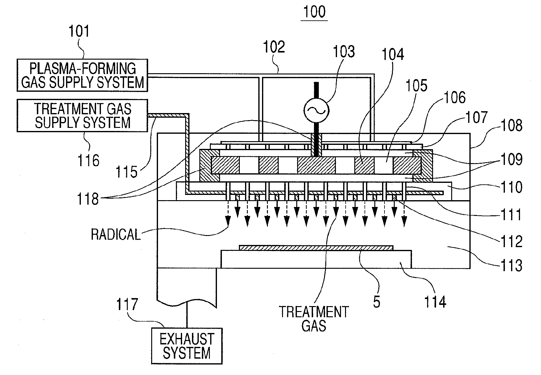
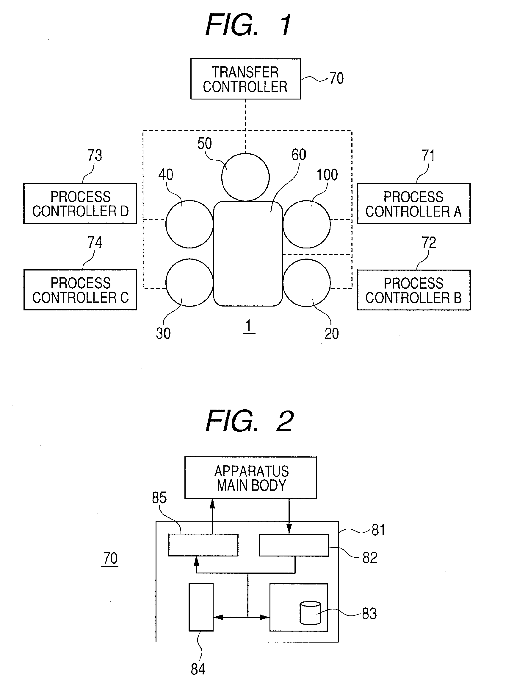
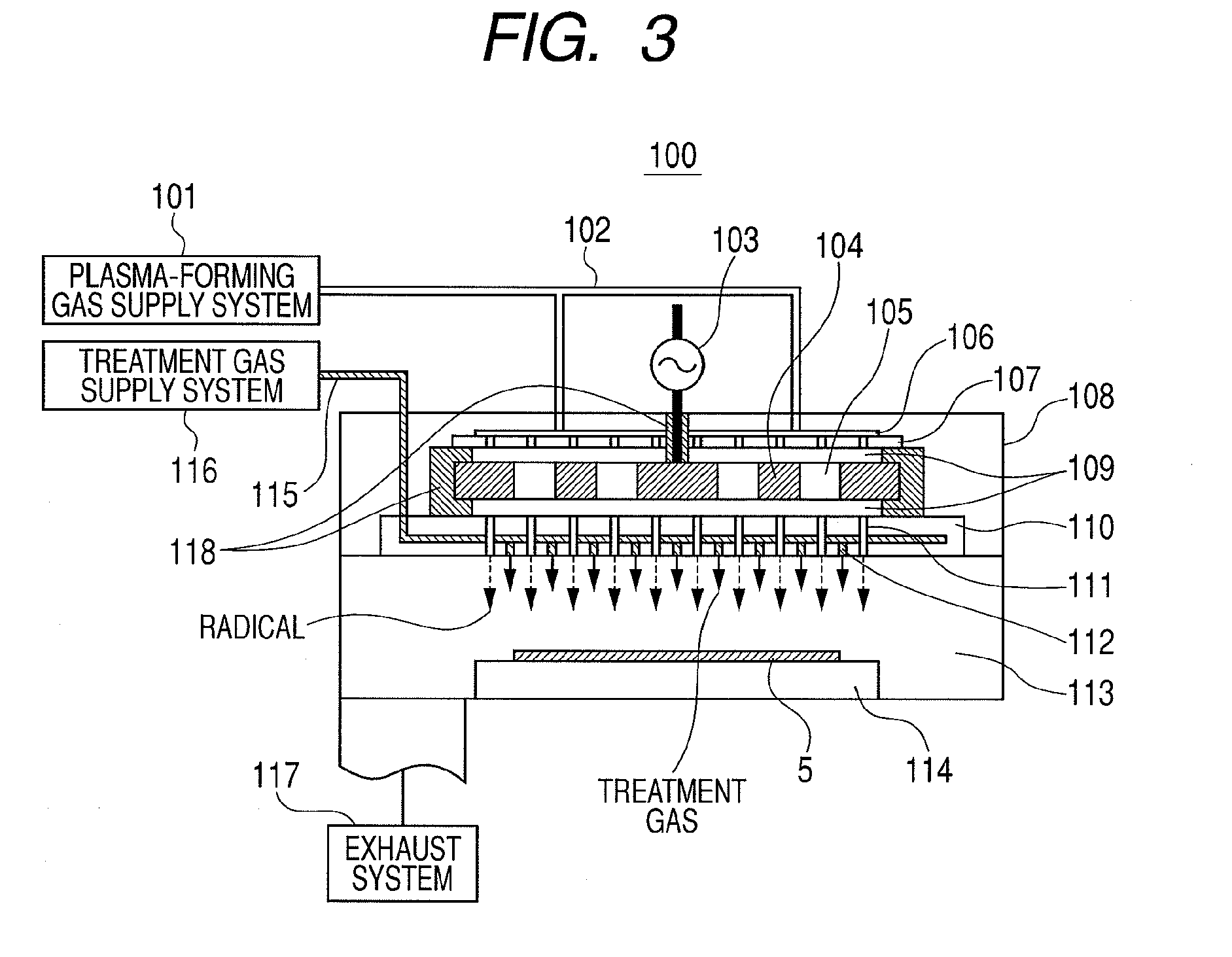
[0052]The examples deal with the cases of applying the present invention to a film-forming apparatus 1 illustrated in FIG. 1, focusing on the process of removing native oxide film and organic matter formed on a Si substrate by the first step using a surface treatment apparatus 100 illustrated in FIG. 3.

[0053]A substrate 5 which is adopted as the sample is a Si single crystal substrate (with 300 mm in diameter) which is allowed to stand in a clean air to form a native oxide film thereon. The substrate 5 is transferred to a load-lock chamber 50 by a substrate transfer mechanism (not shown) to be placed therein. Then, the load-lock chamber 50 is evacuated by an evacuation system (not shown). After evacuating to a desired pressure, or 1 Pa or below, a gate valve (not shown) between the load-lock chamber and the transfer cham...


PUM

PropertyMeasurementUnit
Fractionaaaaaaaaaa
Dielectric polarization enthalpyaaaaaaaaaa
Surfaceaaaaaaaaaa

Abstract

HF-originated radicals generated in a plasma-forming chamber are fed to a treatment chamber via feed holes, while HF gas molecules as the treatment gas are supplied to the treatment chamber from near the radical feed holes to suppress the excitation energy, thereby increasing the selectivity to Si to remove a native oxide film. Even with the dry-treatment, the surface treatment provides good surface flatness equivalent to that obtained by the wet-cleaning which requires high-temperature treatment, and further attains growth of Si single crystal film on the substrate after the surface treatment. The surface of formed Si single crystal film has small quantity of impurities of oxygen, carbon, and the like. After sputtering Hf and the like onto the surface of the grown Si single crystal film, oxidation and nitrification are applied thereto to form a dielectric insulation film such as HfO thereon, thus forming a metal electrode film. All through the above steps, the substrate is not exposed to atmospheric air, thereby suppressing the adsorption of impurities onto the interface, and thus obtaining a C-V curve with small hysteresis. As a result, good device characteristics are obtained in MOS-FET.

Description

CROSS-REFERENCES TO RELATED APPLICATIONS[0001]This application is a continuation application of International Application No. PCT / JP2007 / 071393, filed on Nov. 2, 2007, the entire contents of which are incorporated by reference herein.BACKGROUND OF THE INVENTION[0002]1. Field of the Invention[0003]The present invention relates to an apparatus and a method of manufacturing a semiconductor device, including the treatment of surface of group IV semiconductor.[0004]2. Related Background Art[0005]Conventionally semiconductor Si substrate is subjected to wet-cleaning. The wet-cleaning has, however, problems of failing to completely remove water-marks in dry state, failing to control etching of very thin oxide film, requiring large apparatus, and the like. Furthermore, when the semiconductor substrate is exposed to atmospheric air for a long time after the wet-cleaning, there arise problems of forming native oxide film on the surface thereof and adsorbing carbon atoms thereon to inhibit fil...

Claims


Application Information

Patent Timeline
IPC IPC(8): H01L21/36H01L21/465
CPCH01J37/32091H01L29/66651H01L21/02049H01L21/02532H01L21/02573H01L21/0262H01L21/02658H01L21/28194H01L21/28202H01L29/4916H01L29/495H01L29/4966H01L29/4975H01L29/517H01J37/3244H01L21/302H01L21/02381H01L21/67196
Inventor SEINO, TAKUYAIKEMOTO, MANABUMASHIMO, KIMIKO
Owner CANON ANELVA CORP
Why Eureka
Try Eureka