Circuit and Method for Small Swing Memory Signals

Inactive Publication Date: 2010-10-14
TAIWAN SEMICON MFG CO LTD
View PDF1 Cites 27 Cited by
  • Summary
  • Abstract
  • Description
  • Claims
  • Application Information

AI Technical Summary

Benefits of technology

[0021]An advantage of an embodiment is that by using small swing signal differential voltages on the global bit lines extending across a memory device, the time needed to perform a write cycle in the memory and a read cycle in the memory is reduced.
[0022]A further advantage of an embodiment is that by reducing the amount of signal swing needed to provide signals on the global bit lines of a mem

Problems solved by technology

The prior art global bit lines are full swing signals, and the need to transition these large signal lines from a low voltage level to a high voltage level on such a heavily loaded buss slows memory accesses for both read and

Method used


Image

  • Circuit and Method for Small Swing Memory Signals
  • Circuit and Method for Small Swing Memory Signals
  • Circuit and Method for Small Swing Memory Signals

Examples


Embodiment Construction

[0040]The making and using of the embodiments are discussed in detail below. It should be appreciated, however, that the present invention provides many applicable inventive concepts that can be embodied in a wide variety of specific contexts. The specific embodiments discussed are merely illustrative of specific ways to make and use the invention, and do not limit the scope of the invention.

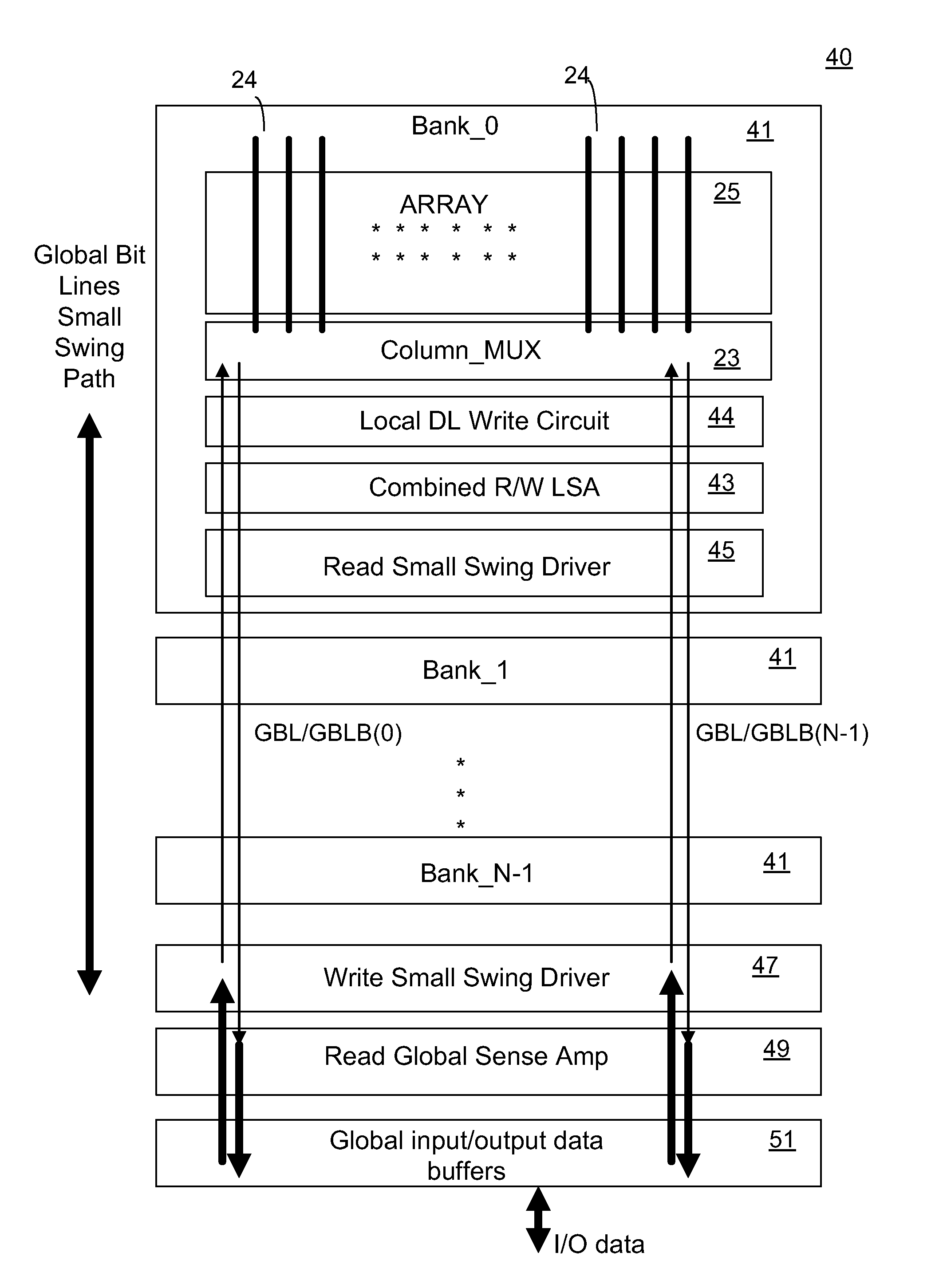
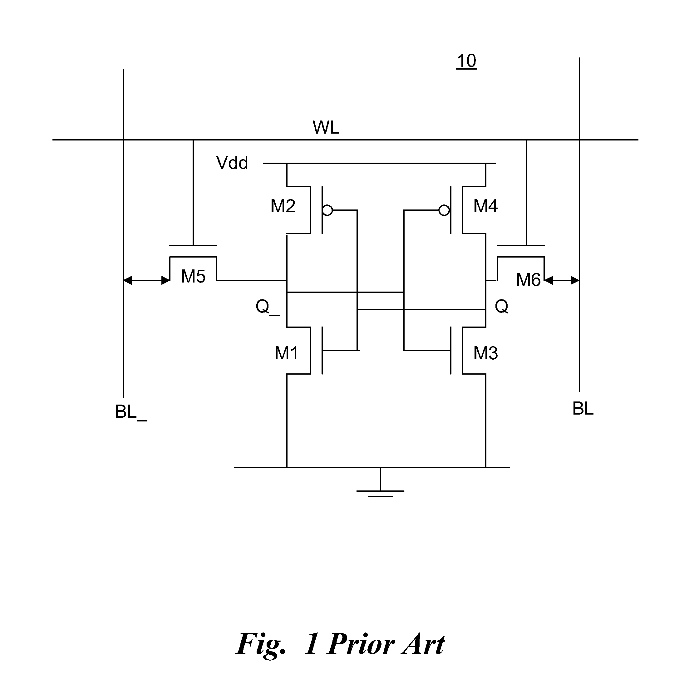
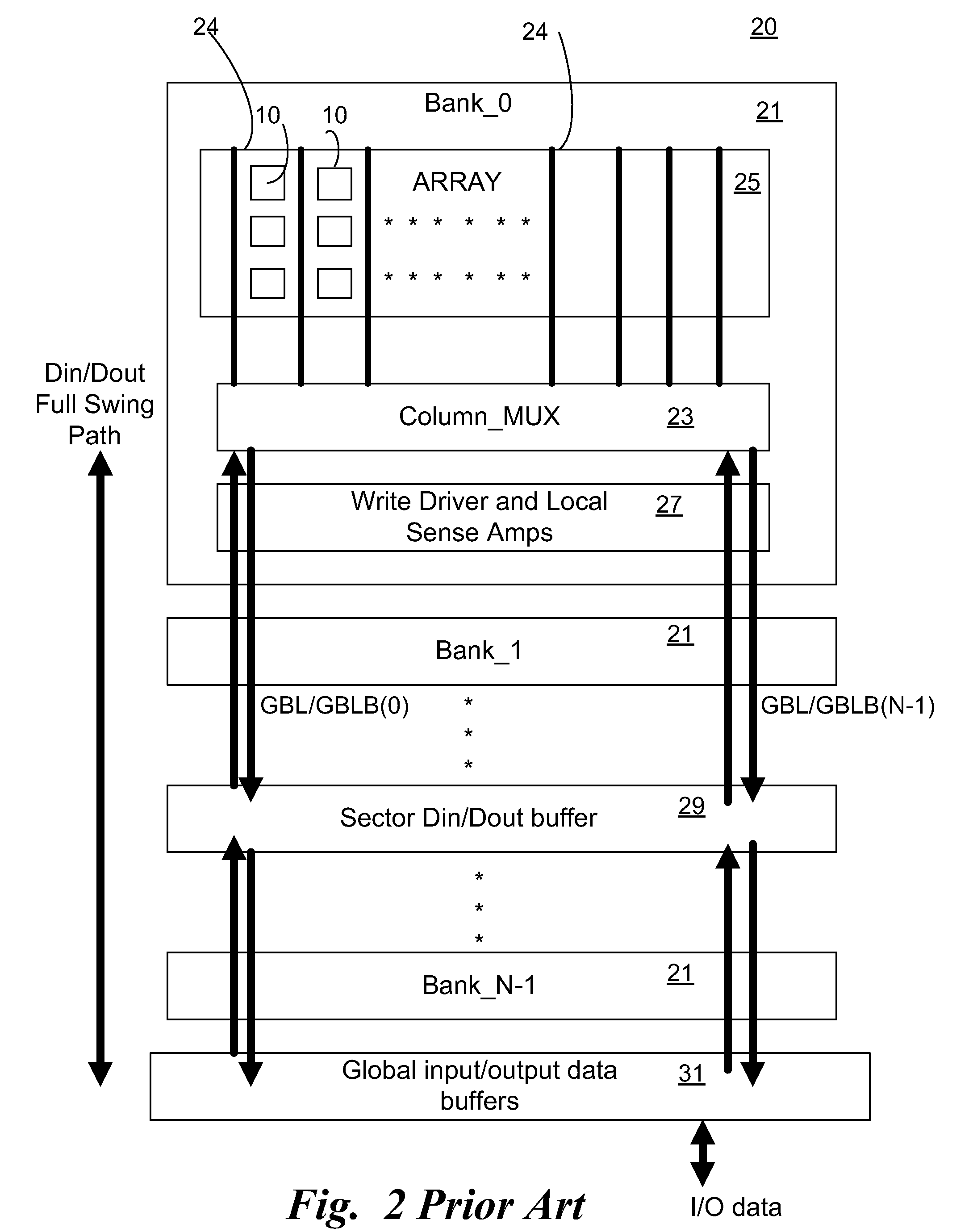
[0041]The embodiments will be described in a specific context, namely a memory device. The memory device can be any memory containing cells where local bit line pairs and local sense amplifiers are used including, as non-limiting examples, DRAM, SRAM, flash and other memory cell types. In the particular embodiments described as illustrative examples herein, an SRAM memory is described. The embodiments may be applied to any memory device formed on a semiconductor substrate, including discrete or standalone memory devices and the embodiments are of particular applicability to embedded memories for...


PUM


Abstract

Circuits and methods for transmitting and receiving small swing differential voltage data to and from a memory are described. A plurality of memory cells is formed in arrays within a plurality of memory banks. Each memory bank is coupled to a pair of small swing differential voltage global bit lines that extend across the memory. A small signal write driver circuit is coupled to the global bit lines and configured to output a small signal differential voltage on the global bit lines during write cycles. A global sense amplifier is coupled to the global bit line pairs and configured to output a full swing voltage on a data line during a read cycle. Methods for providing small swing global bit line signals to memory cells are disclosed. The use of small swing differential voltage signals across the memory reduces power consumption and shortens memory cycle time.

Description

[0001]This application claims the benefit of U.S. Provisional Application No. 61 / 169,087, entitled “Circuit and Method for Small Swing Memory Signals,” filed on Apr. 14, 2009, which is incorporated herein by reference.TECHNICAL FIELD[0002]The present invention relates generally to semiconductor devices, and more particularly to a system and method for providing higher speed and lower power consumption in memory arrays disposed on integrated circuits fabricated on semiconductor devices.BACKGROUND[0003]Semiconductors are used in integrated circuits for a wide range of applications, including personal computers, music and / or video devices, multimedia devices, digital assistants, communications devices, and so forth. In general, integrated circuits include various circuits for providing user desired functionality. Increasingly, memory arrays, once manufactured as stand alone integrated circuits such as commodity DRAM or SRAM integrated circuits, are also being integrated on the same dev...

Claims


Application Information

Patent Timeline
IPC IPC(8): G11C7/02G11C8/00
CPCG11C11/413G11C8/12
Inventor CHEN, YI-TZUSU, CHIA-WEIKUO, MING-ZHANGCHOU, CHUNG-CHENG
Owner TAIWAN SEMICON MFG CO LTD
Why Eureka
Try Eureka