Cluster tool for leds

a technology of leds and clustering tools, which is applied in the direction of crystal growth process, polycrystalline material growth, chemically reactive gas growth, etc., can solve the problems of affecting the practicality of manufacturing, affecting the efficiency of p-doping of such materials, and devices suffering from poor luminescen

Active Publication Date: 2010-10-14
APPLIED MATERIALS INC
View PDF66 Cites 45 Cited by
  • Summary
  • Abstract
  • Description
  • Claims
  • Application Information

AI Technical Summary

Problems solved by technology

While some modestly successful efforts had previously been made in the production of blue LEDs using SiC materials, such devices suffered from poor luminescence as a consequence of the fact that their electronic structure has an indirect bandgap.
While the feasibility of using GaN to create photoluminescence in the blue region of the spectrum has been known for decades, there were numerous barriers that impeded their practical fabrication.
These barriers included the lack of a suitable substrate on which to grow the GaN structures, generally high thermal requirements for growing GaN that resulted in various thermal-convection problems and a variety of difficulties in efficient p-doping of such materials.
The use of sapphire as a substrate was not completely satisfactory because it provides approximately a 15% lattice mismatch with the GaN.
While some improvements have thus been made in the manufacture of such compound nitride semiconductor devices, it is widely recognized that a number of deficiencies yet exist in current manufacturing processes.
Moreover, the high utility of devices that generate light at such wavelengths has caused the production of such devices to be an area of intense interest and activity.

Method used


Image

  • Cluster tool for leds
  • Cluster tool for leds
  • Cluster tool for leds

Examples


example

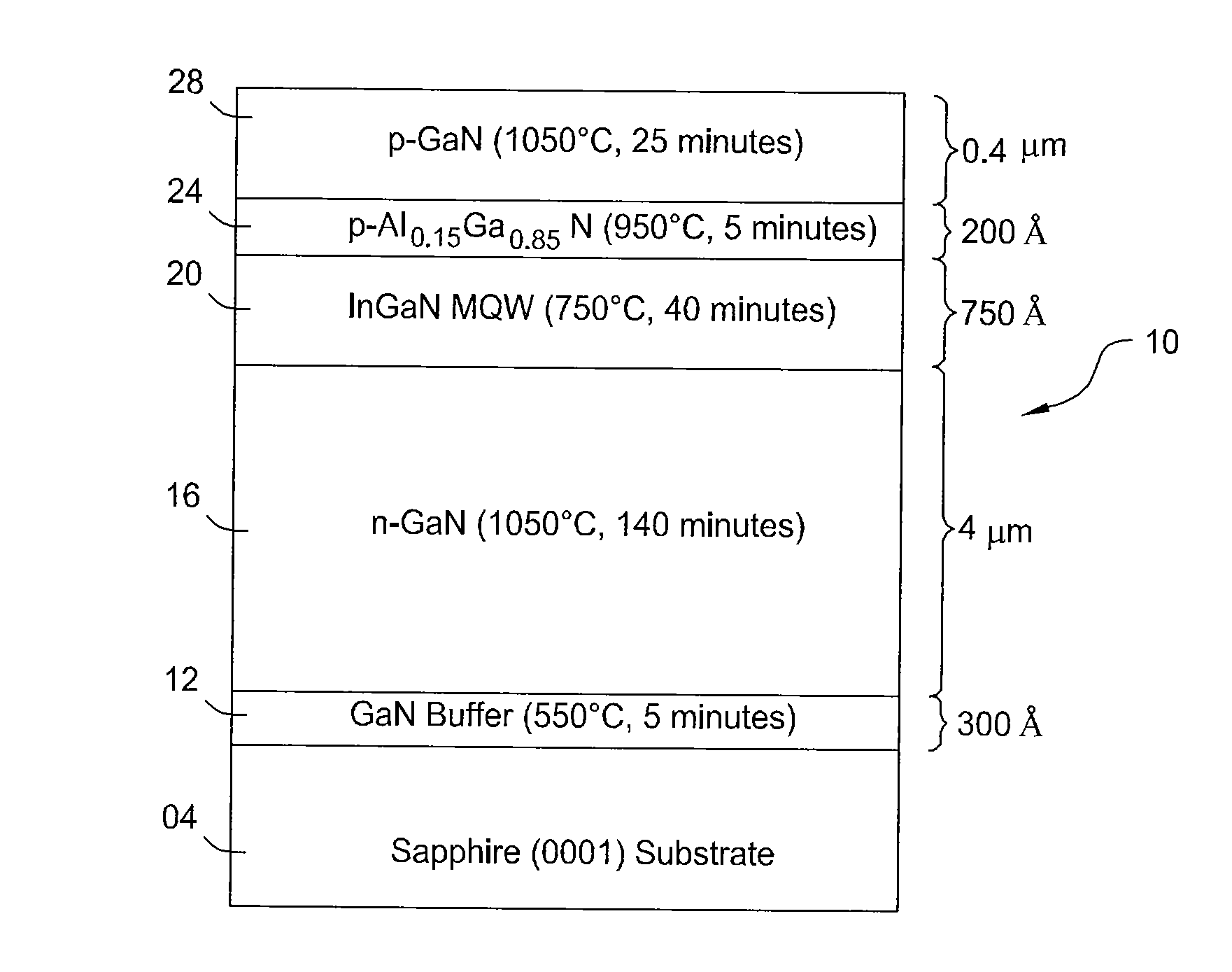
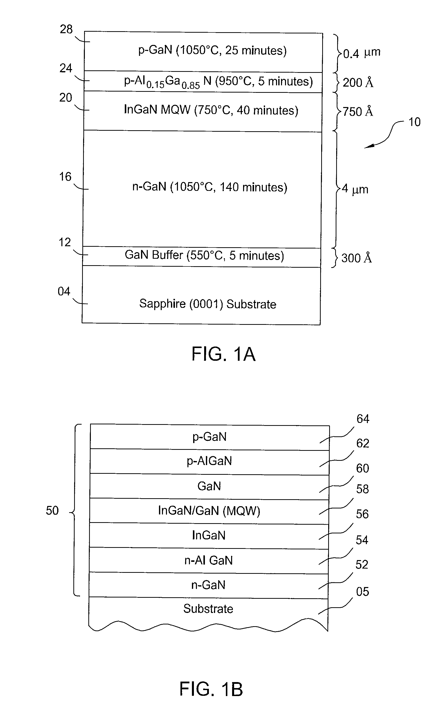
[0125]The following example is provided to illustrate how the general process may be used for the fabrication of compound nitride structures described in connection with the cluster tool 500. The example refers to a LED structure, with its fabrication being performed using the cluster tool 500, wherein the chamber 502 is a HVPE chamber or a MOCVD chamber, and chambers 503, 504 are MOCVD chambers. In one embodiment, the LED structure is similar to structure 10 of FIG. 1A. An overview of the process is provided with the flow diagram of FIG. 7. The deposition of the initial III1-N layers (e.g., the GaN layers) is performed either in the chamber 502 by a MOCVD process or a HVPE process, deposition of III2-N layers (e.g., the InGaN layer) is performed in the second MOCVD chamber 503, and deposition of the III3-N layers (e.g. the AlGaN, and GaN contact layers) is performed in the third MOCVD chamber 504.

[0126]At block 1602 one or more sapphire substrates are transferred into the first sub...


PUM

PropertyMeasurementUnit
temperatureaaaaaaaaaa
thicknessaaaaaaaaaa
temperatureaaaaaaaaaa

Abstract

The present invention generally provides apparatus and methods for forming LED structures. One embodiment of the present invention provides a method for fabricating a compound nitride structure comprising forming a first layer comprising a first group-III element and nitrogen on substrates in a first processing chamber by a hydride vapor phase epitaxial (HVPE) process or a metal organic chemical vapor deposition (MOCVD) process, forming a second layer comprising a second group-III element and nitrogen over the first layer in a second processing chamber by a MOCVD process, and forming a third layer comprising a third group-III element and nitrogen over the second layer by a MOCVD process.

Description

CROSS-REFERENCE TO RELATED APPLICATIONS[0001]This application claims priority to U.S. Provisional Patent Application Ser. No. 61 / 177,098 (Attorney Docket 13986L), filed on May 11, 2009, U.S. Provisional Patent Application Ser. No. 61 / 230,877 (Attorney Docket 14243L03), filed on Aug. 3, 2009, U.S. Provisional Patent Application Ser. No. 61 / 173,536 (Attorney Docket 14349L), filed on Apr. 28, 2009, U.S. Provisional Patent Application Ser. No. 61 / 168,399 (Attorney Docket 14243L), filed on Apr. 10, 2009, and U.S. Provisional Patent Application Ser. No. 61 / 168,630 (Attorney Docket 14243L02), filed on May 24, 2009. All aforementioned applications are incorporated herein by reference.BACKGROUND OF THE INVENTION[0002]1. Field of the Invention[0003]Embodiments of the present invention generally relate to the manufacture of semiconductor devices. More particularly, embodiments of the present invention relate to apparatus and method for manufacturing nitride compound semiconductor device, such ...

Claims


Application Information

Patent Timeline
Patent Type & Authority Applications(United States)
IPC IPC(8): H01L21/205
CPCC30B25/02C30B29/406H01L21/0242H01L21/02458H01L21/0254H01L33/007H01L21/67109H01L21/67115H01L21/67167H01L21/67207H01L21/0262
Inventor NIJHAWAN, SANDEEPBURROWS, BRIAN H.ISHIKAWA, TETSUYAKRYLIOUK, OLGAVASUDEV, ANANDSU, JIEQUACH, DAVID H.CHANG, ANZHONGMELNIK, YURIYRATIA, HARSUKHDEEP S.NGUYEN, SON T.PANG, LILY
Owner APPLIED MATERIALS INC
Why Eureka
Try Eureka