Eureka AIR delivers breakthrough ideas for toughest innovation challenges, trusted by R&D personnel around the world.

Organic Thin Film Transistors, Active Matrix Organic Optical Devices and Methods of Making the Same

Inactive Publication Date: 2010-10-21
CAMBRIDGE DISPLAY TECH LTD
View PDF12 Cites 8 Cited by
  • Summary
  • Abstract
  • Description
  • Claims
  • Application Information

AI Technical Summary

Benefits of technology

[0014]In order to solve this problem, the present applicant has found it advantageous to treat the surface of the well-defining bank in order to reduce its wettability prior to depositing the OSC from solution. A de-wetting surface on the top of the well-defining bank layer aids in containing the OSC within the well when it is deposited.
[0016]In light of the above, in accordance with a particularly preferred embodiment of the present invention there is provided a method of manufacturing an organic thin film transistor, comprising: providing a substrate comprising source and drain electrodes defining a channel region; forming a patterned layer of insulting material defining a well surrounding the channel region; depositing a protective layer in the well; subjecting exposed portions of the patterned layer of insulating material to a de-wetting treatment to lower the wettability of the exposed portions; removing the protective layer; and depositing organic semiconductive material from solution into the well.
[0017]The advantage of the aforementioned method is that by providing a protective layer in the well, the de-wetting treatment can be performed after well formation while protecting underlying layers in the well.
[0020]Preferably, the protective layer is a resist material, most preferably a positive-acting resist. Preferably, the well-defining bank material is also a resist material, but most preferably a negative-acting resist. The protective layer is preferably patterned using the same mask as that used to pattern the well-defining bank layer. By using opposite acting resists for the protective layer and the well-defining bank layer, both layers can be deposited using the same mask and no further mask is needed for the extra lithographic steps involved in forming the protective layer. Of course, it is also possible to achieve the same effect for two positive-acting photoresists (or two negative-acting photoresists) by employing two different masks.

Problems solved by technology

The present applicant has found that even if a patterned layer of well-defining bank material is provided, problems still exist in containing the OSC within the channel region and providing good film formation of the OSC in the channel region using solution processing techniques for deposition of the OSC.
Uncontrollable wetting of the well-defining bank material occurs since the contact angle of organic solvents in which the OSC is typically deposited is low.
In the worst case the OSC may overspill the well.
However, the present applicant has found that there are some problems associated with both these possibilities.
Treatments to reduce the wettability of the insulating layer are generally unstable and the treated surface tends to revert to its original wettability over a period of time, particularly if subjected to further processing steps.
Alternatively, if the well is formed first and then a surface treatment is applied, such surface treatments have been found to damage the active layers of the OTFT exposed in the well.
It has been found that in bottom gate devices, the dielectric layer which is exposed when the well is formed is particularly sensitive to de-wetting treatments.
Furthermore, for both top and bottom gate devices, source and drain electrodes will be exposed after well formation and the de-wetting treatments can detrimentally affect the contact formed between these electrodes and a subsequently deposited OSC.

Method used


Image

  • Organic Thin Film Transistors, Active Matrix Organic Optical Devices and Methods of Making the Same
  • Organic Thin Film Transistors, Active Matrix Organic Optical Devices and Methods of Making the Same
  • Organic Thin Film Transistors, Active Matrix Organic Optical Devices and Methods of Making the Same

Examples


Embodiment Construction

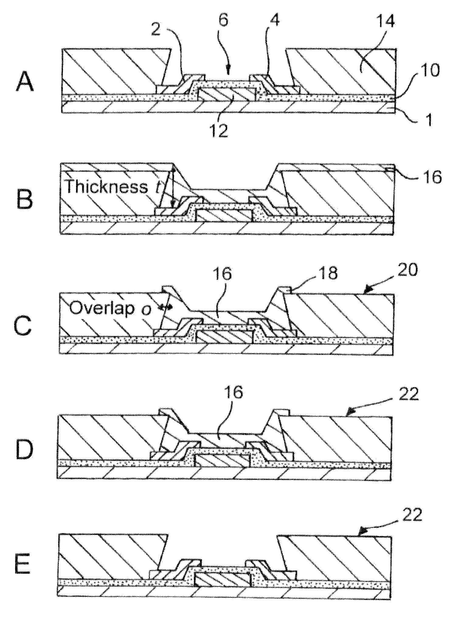
[0035]Embodiments of the present invention introduce an additional resist patterning step into the OTFT process flow to protect the sensitive gate dielectric from damage during the surface treatment of the well-defining bank material prior to OSC deposition. In the preferred embodiments this is done without the need for an additional resist mask. Thus embodiments have the potential for obtaining good OTFT performance whilst retaining optimum printing performance during OSC deposition.

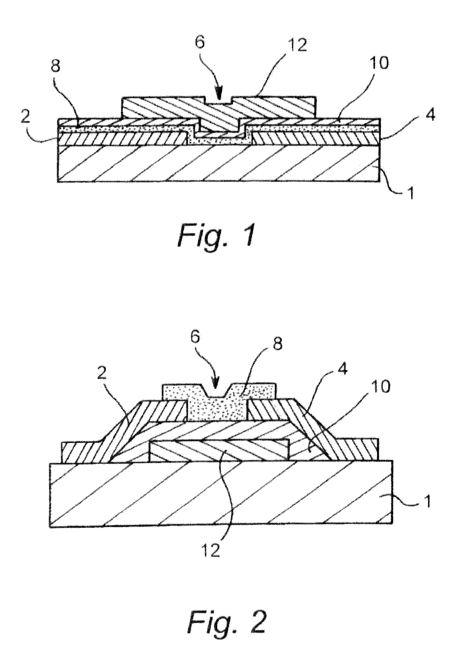
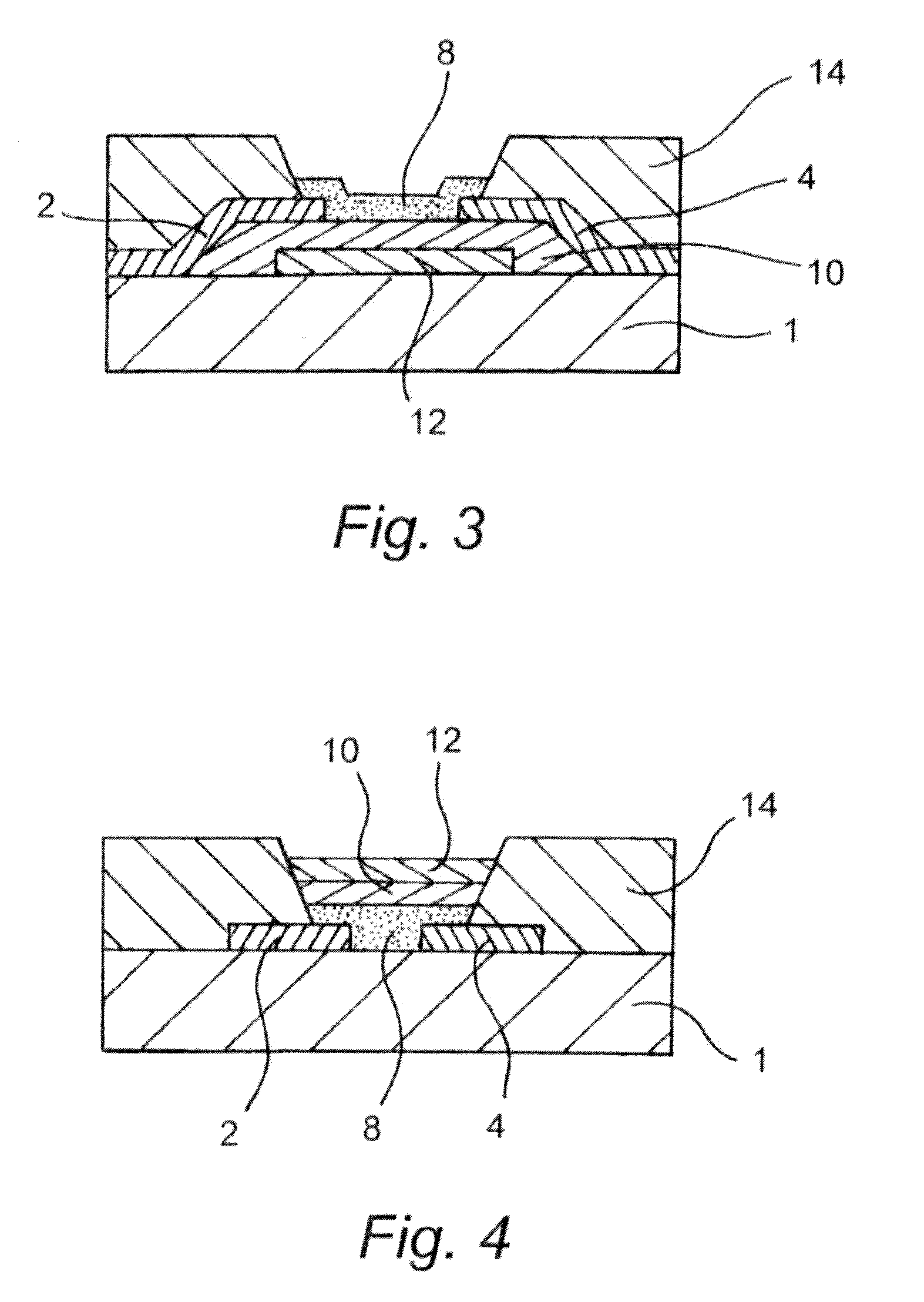
[0036]FIG. 5 shows the method steps involved in forming a bottom-gate organic thin film transistor according to an embodiment of the present invention. Like reference numerals to those used in FIGS. 1 to 4 have been used for corresponding parts. FIG. 5(A) depicts the device structure under development prior to OSC deposition. This structure is formed by depositing a gate electrode 12 on a substrate 1, depositing a gate dielectric 10 over the gate electrode 12, depositing source and drain electrodes 2, 4...


PUM


Abstract

A method of manufacturing an organic thin film transistor, comprising: providing a substrate comprising source and drain electrodes defining a channel region; forming a patterned layer of insulting material defining a well surrounding the channel region; depositing a protective layer in the well; subjecting exposed portions of the patterned layer of insulating material to a de-wetting treatment to lower the wettability of the exposed portions; removing the protective layer; and depositing organic semiconductive material from solution into the well.

Description

FIELD OF INVENTION[0001]The present invention relates to organic thin film transistors active matrix organic optical devices and methods of making the same.BACKGROUND OF THE INVENTION[0002]Transistors can be divided into two main types: bipolar junction transistors and field-effect transistors. Both types share a common structure comprising three electrodes with a semi-conductive material disposed there between in a channel region. The three electrodes of a bipolar junction transistor are known as the emitter, collector and base, whereas in a field-effect transistor the three electrodes are known as the source, drain and gate. Bipolar junction transistors may be described as current-operated devices as the current between the emitter and collector is controlled by the current flowing between the base and emitter. In contrast, field-effect transistors may be described as voltage-operated devices as the current flowing between source and drain is controlled by the voltage between the ...

Claims


Application Information

Patent Timeline
IPC IPC(8): H01L51/10H01L51/40H01L33/00
CPCH01L27/3295H01L51/0545H01L51/0541H01L51/0003H10K59/122H10K71/12H10K10/464H10K10/466
Inventor BALE, MARKHATCHER, MICHAEL
Owner CAMBRIDGE DISPLAY TECH LTD
Why Eureka
Eureka Blog
Learn More