This helps you quickly interpret patents by identifying the three key elements:
Problems solved by technology
Method used
Benefits of technology
Benefits of technology
[0017]Therefore, it is an object of the present invention to provide a photoelectric conversion module in which an optical device and an optical waveguide are aligned in a horizontal direction, thereby increasing the optical coupling efficiency and thus decreasing light loss.
[0018]It is another object of the present invention to provide a photoelectric conversion module in which an electric circuit device and an optical circuit device are independently separated from each other and positioned on a printed circuit board, thereby independently replacing the electric circuit device or the optical circuit device when it malfunctions and therefore simplifying repairs.
[0019]It is another object of the present invention to provide a photoelectric conversion module in which the number of constituent elements of the photoelectric conversion module is decreased, compared with that of the conventional photoelectric conversion module, thereby enabling mass production and decreasing the manufacturing cost.
Problems solved by technology
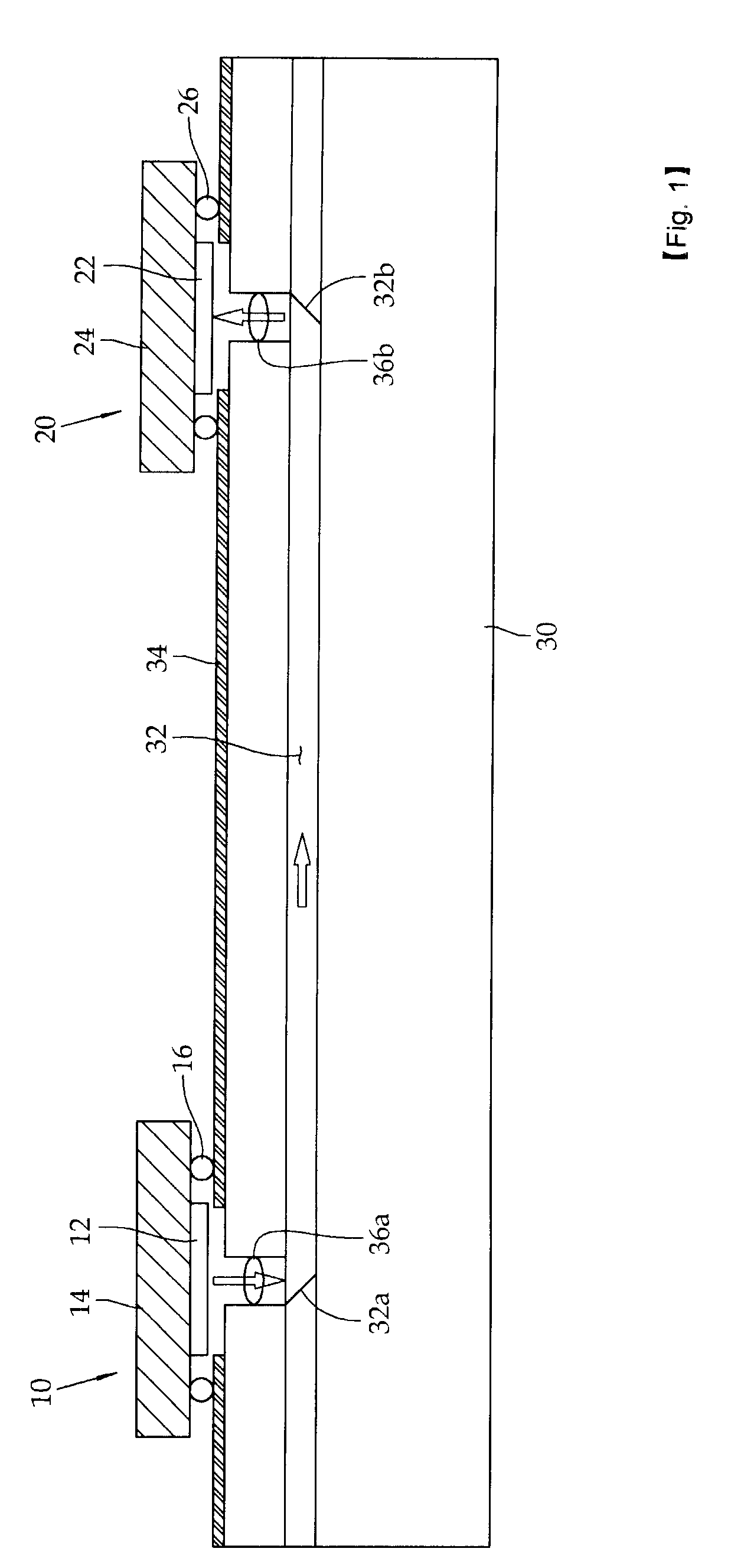
However, since the number of the lenses 36a and 36b to be positioned is increased according to the distance between the first and second optical devices 12 and 22 and the optical waveguide 32, there are the problems in that an additional process is needed to position the lenses 36a and 36b between the first and second optical devices 12 and 22 and the optical waveguide 32 and this additional process becomes an obstacle in mass production.
Moreover, the reliability of the photoelectric conversion module is greatly decreased during this process.
As described above, in the conventional photoelectric conversion module, since the optical coupling efficiency is decreased by the vertical distance between the optical devices and the optical waveguide, light loss is caused when light is emitted or received.
Moreover, since the micro mirrors, lenses and the like are additionally formed or positioned to solve the problem in that the optical coupling efficiency is decreased, the process of manufacturing the photoelectric conversion module becomes complicated.
Moreover, since the devices, such as the micro mirrors, are manufactured in a micro-miniature structure, in fact, not only it is difficult to match the devices with the optical axis but also the devices are easily damaged during the manufacturing process.
Consequently, both process and production costs increase.
Method used
Image
Click on the blue label to locate the original text in one second.
Reading with bidirectional positioning of images and text.
Examples
embodiment 1
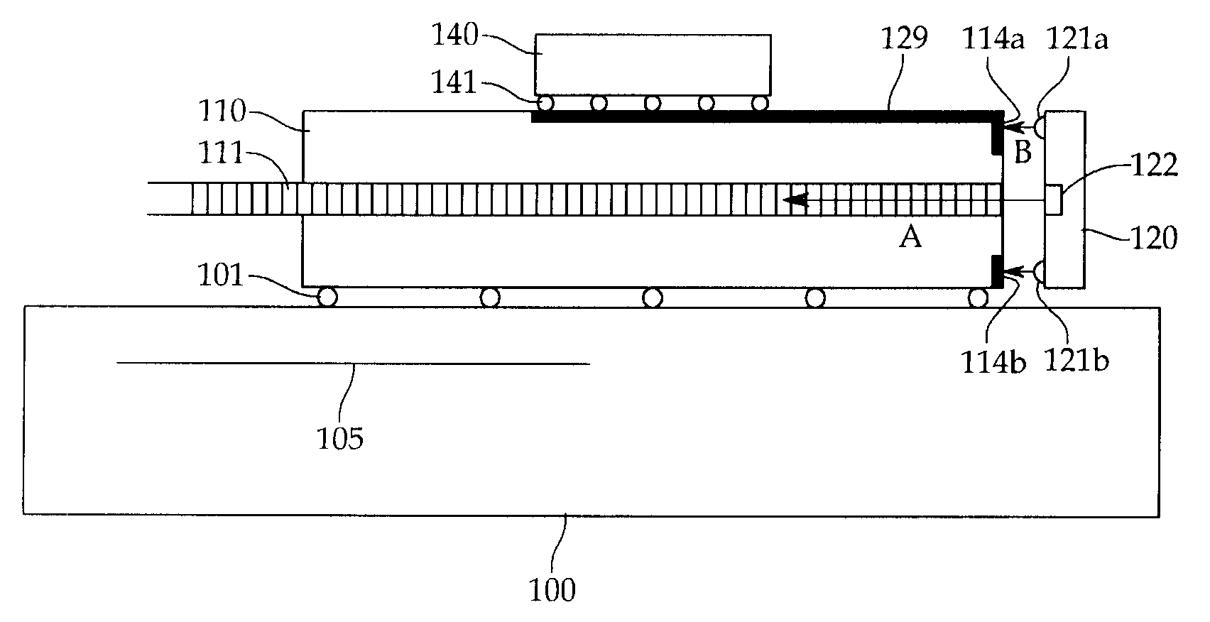
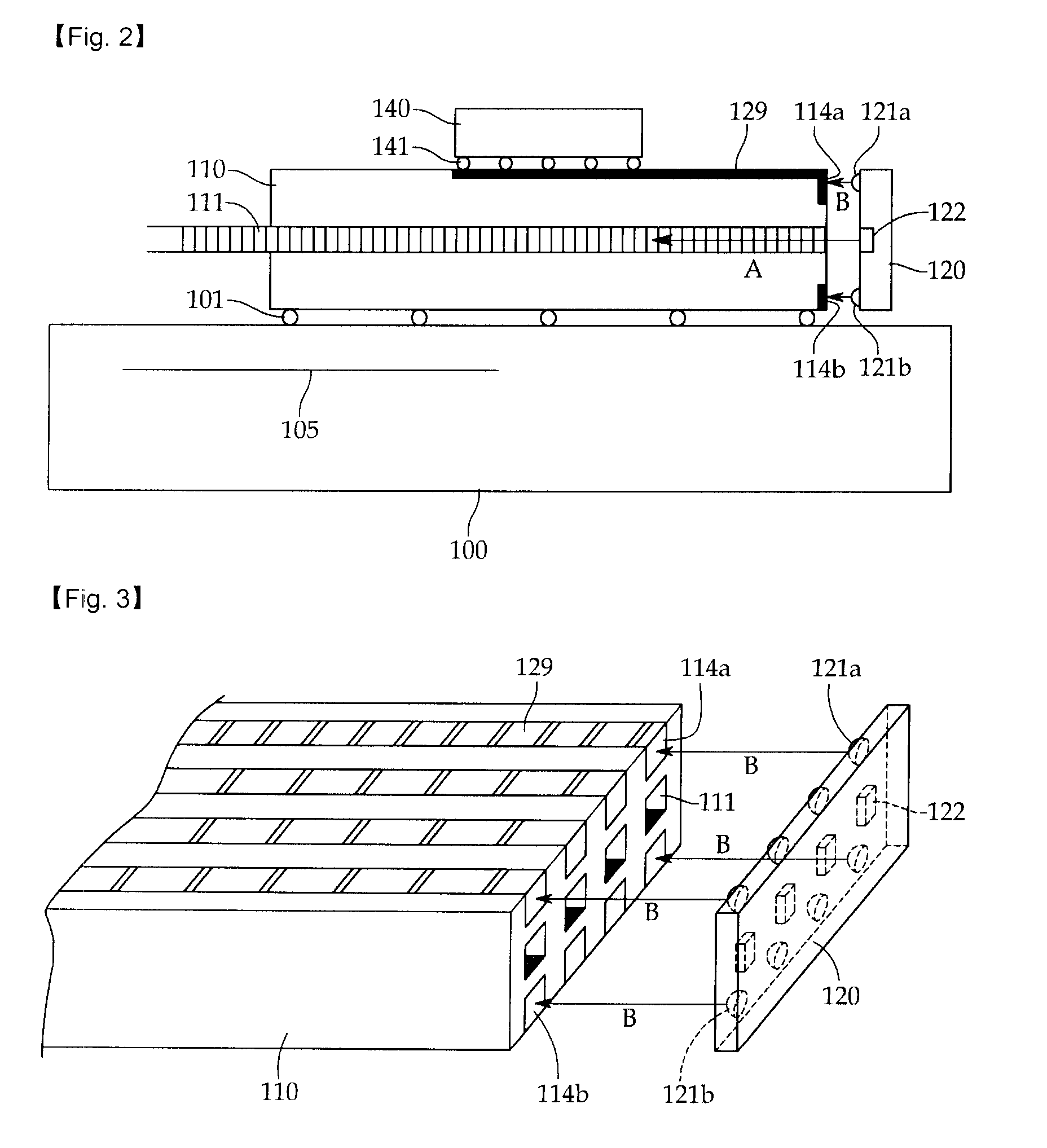
[0050]FIG. 2 is a sectional view illustrating a photoelectric conversion module is according to a first embodiment of the present invention.
[0051]As illustrated in FIG. 2, the photoelectric conversion module according to the first embodiment of the present invention comprises: a printed circuit board 100, an integrated circuit (IC) board 110 mounted on the printed circuit board 100 and including an optical waveguide array 111 inside, a semiconductorchip 140 mounted on the integrated circuit board 110, and an optical device array 120 positioned horizontally with the optical waveguide array 111.
[0052]The integrated circuit board 110 is electrically connected to the printed circuit board 100 by a flip chip bonding method using a first connection bump 101. The optical waveguide array 111 positioned in the integrated circuit board 110 is to transmit an optical signal provided from the optical device array 120.
[0053]FIG. 3 is a perspective view illustrating the integrated circuit board 1...
embodiment 2
[0070]FIG. 5 is a sectional view illustrating a photoelectric conversion module according to a second embodiment of the present invention.
[0071]As illustrated in FIG. 5, the photoelectric conversion module according to the second embodiment of the present invention has a similar structure to the photoelectric conversion module according to the first embodiment of the present invention illustrated in FIG. 2, except for a first optical device array 220a and a second optical device array 220b connected to both sides of an integrated circuit board 210.
[0072]In the photoelectric conversion module according to the second embodiment of the present invention, the integrated circuit board 210 is bonded on a printed circuit board 200, by a flip chip bonding method through a first connection bump 201. A signal line 229 is formed on the integrated circuit board 210, to transmit electric signals from a first semiconductorchip 240a and a second semiconductor chip 240b. A first electrode pad 214a...
embodiment 3
[0079]FIG. 6 is a sectional view illustrating a photoelectric conversion module according to a third embodiment of the present invention.
[0080]Referring to FIG. 6, the photoelectric conversion module according to the third embodiment of the present invention has a similar structure to the photoelectric conversion module according to the second embodiment of the present invention, except that a first integrated circuit board 310a and a second integrated circuit board 310b are mounted on a printed circuit board 300, and a first optical device array 320a and a second optical device array 320b are respectively positioned at sides of the first and second integrated circuit boards 310a and 310b facing each other.
[0081]As illustrated in FIG. 6, the first and second integrated circuit boards 310a and 310b are positioned on the printed circuit board 300 so as to be spaced apart from each other. The first and second integrated circuit boards 310a and 310b are connected to each other by an opt...
PUM
Abstract
There is provided a photoelectric conversion module in which an optical device and an optical waveguide are arrayed in a horizontal direction, thereby improving the optical coupling efficiency and therefore, reducing light loss. To this end, the present invention provides a photoelectric conversion module comprising: a printed circuit board; an integrated circuit board mounted on the printed circuit board, wherein an optical waveguide array is positioned within the integrated circuit board so as to pass from one side to the other side of the integrated circuit board, and first and second electrode pads are positioned at one sidewall of the integrated circuit board; an optical device array wherein first and second electrode bumps to be respectively connected to the first and second electrode pads are positioned at one sidewall of the optical device array facing the integrated circuit board and an optical device is positioned in a middle part of the optical device array; and a semiconductorchip mounted on the is integrated circuit board.
Description
CROSS-REFERENCE TO RELATED APPLICATION[0001]This application claims the benefit of Korean Patent Application No. 10-2009-0035363, filed Apr. 23, 2009, and No. 10-2009-0056421 filed Jun. 24, 2009, the disclosure of which is hereby incorporated herein by reference in its entirety.BACKGROUND OF THE INVENTION[0002]1. Field of the Invention[0003]The present invention relates to a photoelectric conversion module, and more particularly, to a photoelectric conversion module which improves the optical coupling efficiency.[0004]2. Description of the Related Art[0005]In the present information and communication technologies, optical communication technologies are developed to achieve high speed communication environments according to high speed and high capacity data transmission. In the optical communication, a photoelectric conversion device of a sender converts an electric signal into an optical signal, and the converted optical signal is transmitted to a receiver by an optical fiber or an ...
Claims
Application Information
Patent Timeline
Application Date:The date an application was filed.
Publication Date:The date a patent or application was officially published.
First Publication Date:The earliest publication date of a patent with the same application number.
Issue Date:Publication date of the patent grant document.
PCT Entry Date:The Entry date of PCT National Phase.
Estimated Expiry Date:The statutory expiry date of a patent right according to the Patent Law, and it is the longest term of protection that the patent right can achieve without the termination of the patent right due to other reasons(Term extension factor has been taken into account ).
Invalid Date:Actual expiry date is based on effective date or publication date of legal transaction data of invalid patent.

