Magnetoresistance device including layered ferromagnetic structure, and method of manufacturing the same

a ferromagnetic structure and magnetoresistance technology, applied in the field of magnetoresistance devices, can solve the problems of difficult to reverse the magnetization inability to achieve the effect of enhancing the crystalline orientation of the first non-magnetic layer, and increasing the volume of the free magnetic layer undetectedly

Active Publication Date: 2010-11-04
NEC CORP
View PDF34 Cites 36 Cited by
  • Summary
  • Abstract
  • Description
  • Claims
  • Application Information

AI Technical Summary

Benefits of technology

[0134]The tunnel barrier layer 5 is composed of a very thin non-magnetic insulative layer. In this embodiment, many materials may be used for the tunnel barrier layer 5. In an aspect of the crystalline structure, the tunnel barrier layer 5 may be formed of amorphous or crystalline material. Specifically, the tunnel barrier layer 5 may be composed of an amorphous AlOx layer formed by oxidizing an aluminum film. Alternatively, a highly-oriented crystalline MgO layer having the NaCl structure may be used as the tunnel barrier layer 5. The use of a crystalline MgO layer exhibiting high (001) orientation as the tunnel barrier layer 5 advantageously achieves a high MR ratio of the magnetic tunnel junction. It should be noted that the present invention causes its advantageous effects, regardless of the material and crystalline structure of the tunnel barrier layer 5.
[0135]The free magnetic layer 6 is composed of an SAF including ferromagnetic layers having reversible magnetizations. The magnetizations of the free magnetic layer 6 are directed in the direction corresponding to data to be stored. The fixed magnetic layer 4, the tunnel barrier layer 5 and the free magnetic layer 6 constitute an MTJ element. The resistance of the MTJ element changes on the direction of the magnetizations of the ferromagnetic layers within the free magnetic layer 6, that is, the data stored onto the free magnetic layer 6, due to the tunnel magnetoresistance effect. The data is identified on the basis of the change in the resistance of the MTJ element.
[0136]Specifically, the free magnetic layer 6 is composed of a first ferromagnetic layer 11, a second ferromagnetic layer 13, and a non-magnetic layer 12 placed therebetween. The first ferromagnetic layer 11 is formed on the tunnel barrier layer 5. The first and second ferromagnetic layers 11 and 13 are both configured to exhibit the ferromagnetic behavior. The non-magnetic layer 12 is configured to provide the antiferromagnetic exchange coupling between the first and second ferromagnetic layers 11 and 13. In detail, the material and film thickness of the non-magnetic layer 12 are selected so that the first and second ferromagnetic layers 11 and 13 are antiferromagnetically coupled. In a preferred embodiment, the non-magnetic layer 12 is composed of a Ru film having a thickness of about 0.9 nm. As described below in detail, the MRAM structure in this embodiment addresses improving the crystal orientation of the non-magnetic layer 12. The improvement of the crystalline orientation of the non-magnetic layer 12 is important in order to enhance the exchange coupling between the first and second ferromagnetic layers 11 and 13.
[0137]In the MRAM structure of FIG. 5A, the first ferromagnetic layer 11 is composed of two ferromagnetic films 21, 23, and a buffer film 22 placed therebetween. The ferromagnetic films 21 and 23 are made of ferromagnetic material, such as permalloy (NiFe), and CoFe. The material and deposition method of the buffer film 22 are selected so that the crystalline orientation of the ferromagnetic film 23 deposited thereon is enhanced. The buffer film 22 allows the ferromagnetic film 23 to exhibit crystalline orientation higher than that of the ferromagnetic film 21, which is located below the buffer film 22. The improvement of the crystalline orientation of the ferromagnetic film 23 leads to the improvement of the crystalline orientation of the non-magnetic layer 12 formed thereon, and thereby effectively enhances the exchange coupling between the first and second ferromagnetic layers 11 and 13. The buffer film 22 may be formed of tantalum or ruthenium through a sputtering method. The details of the buffer film 22 will be described later.
[0138]The improvement of the crystalline orientation of the ferromagnetic film 23 by the buffer film 22 is essentially important for enhancing the exchange coupling between the first and second ferromagnetic layers 11 and 13. The ferromagnetic film 21 exhibits poor crystalline orientation, since being formed on the tunnel barrier layer 5 that is amorphous. The buffer film 22 effectively avoids the non-magnetic layer 12 being poorly-oriented because of the poor crystalline orientation of the ferromagnetic film 21. The buffer film 22 formed on the ferromagnetic film 21 improves the crystalline orientation of the ferromagnetic film 23 formed thereon and consequently improves the crystalline orientation of the non-magnetic layer 12 formed on the ferromagnetic film 23. The improvement in the crystalline orientation of the non-magnetic layer 12 effectively enhances the exchange coupling between the first and second ferromagnetic layers 11 and 13.
[0139]The buffer film 22 is formed so that the ferromagnetic films 21 and 23 are antiferromagnetically coupled. It should be noted that the configuration in which, the first ferromagnetic layers 11 functions as a single ferromagnetic layer, although incorporating the multiple ferromagnetic films 21 and 23.

Problems solved by technology

However, in the MRAM that uses a single-layered ferromagnetic film as the free magnetic layer, the increase in the volume of the free magnetic layer undesirably increases the magnetization and thickness product (namely, the product of the magnetic film thickness and the saturation magnetization) of the free magnetic layer. as the free magnetic layer.
The increase in the magnetization and thickness product of the free magnetic layer increases the magnetic field generated by the magnetization, and thereby undesirably causes the magnetic interference between adjacent memory cells.
Moreover, the increase in the magnetization and thickness product of the free magnetic layer makes it hard to reverse the magnetization of the free magnetic layer.
Achieving sufficiently great exchange coupling may be a problem, especially in the case where a layered ferromagnetic structure is formed on a tunnel barrier layer.
As a result, a ferromagnetic layer formed on the tunnel barrier layer often exhibits poor orientation.
This weakens the exchange coupling between the ferromagnetic layers, and prevents desired properties from being achieved in the layered ferromagnetic structure.
Such situation is especially severe when the ferromagnetic layers within the SAF are formed of NiFe.
It is hard to obtain sufficiently large exchange coupling between NiFe ferromagnetic layers within SAF.
In such situations, large exchange coupling is not obtained, which causes the same problem.
In many cases, crystal structures of SAF films are not well matched with that of the underlying crystalline tunnel barrier film.
Although there is a need for a technique that achieves improved crystal growth of SAF films regardless of the crystal structure the underlying tunnel barrier, no approach has been currently proposed.
Incorporating a layer structure composed of CoFe and NiFe films within each ferromagnetic layer of the SAF may achieve enhanced exchange coupling; however, the use of CoFe films results in the increase in the saturated magnetization and crystal magnetic anisotropy of the SAF.
However, the excessive increase in the exchange coupling energy J undesirably leads to the increase in the spin flop field Hflop.
This implies that the magnitude of the exchange coupling energy is not freely controllable by the thickness of the non-magnetic layer.
The disclosed SAF structure, however, does not address enhancing or controlling the exchange coupling energy.

Method used


Image

  • Magnetoresistance device including layered ferromagnetic structure, and method of manufacturing the same
  • Magnetoresistance device including layered ferromagnetic structure, and method of manufacturing the same
  • Magnetoresistance device including layered ferromagnetic structure, and method of manufacturing the same

Examples


first embodiment

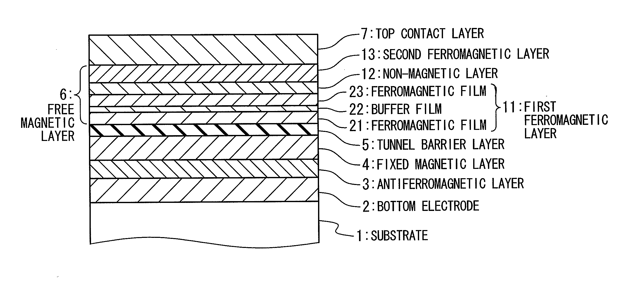
[0133]FIG. 5A is a sectional view showing an exemplary structure of MRAM memory cells in a first embodiment of the present invention. An MRAM is composed of a substrate 1, a bottom electrode 2 formed on the substrate 1, an antiferromagnetic layer 3 formed of antiferromagnetic material, a fixed magnetic layer 4, a tunnel barrier layer 5, a free magnetic layer 6 and a top contact layer 7. The antiferromagnetic layer 3 fixes the magnetization of the fixed magnetic layer 4 by exchange interaction therebetween. The fixed magnetic layer 4 is composed of a single ferromagnetic layer or an SAF, and the magnetization(s) thereof is fixed by the antiferromagnetic layer 3.

[0134]The tunnel barrier layer 5 is composed of a very thin non-magnetic insulative layer. In this embodiment, many materials may be used for the tunnel barrier layer 5. In an aspect of the crystalline structure, the tunnel barrier layer 5 may be formed of amorphous or crystalline material. Specifically, the tunnel barrier lay...

second embodiment

[0160]One issue of the structure of the free magnetic layer 6 shown in FIG. 5A is the difference in the characteristics between the first and second ferromagnetic layers 11 and 13 resulting from the structure difference therebetween. The large difference in the characteristics between the first and second ferromagnetic layers 11 and 13, especially, the large difference in the crystal magnetic anisotropy and the magnetization-and-thickness product is undesirable for implementing the toggle writing.

[0161]In a second embodiment, a technique is provided for reducing the difference in the characteristics between the first and second ferromagnetic layers 11 and 13. Specifically, in the second embodiment, as shown in FIG. 8, the second ferromagnetic layer 13 is composed of a plurality of ferromagnetic films 26, 28, and a buffer film 27 placed therebetween. It should be noted that the structure of the first ferromagnetic layer 11 may be any of the structures shown in FIGS. 5A, 5B, 7A and 7B...

third embodiment

[0170]In a third embodiment, a technique is provided in which three or more ferromagnetic layers are incorporated within the free magnetic layer 6. The increase in the number of the ferromagnetic layers within free magnetic layer 6 is effective for avoiding undesirable magnetization reversal of the free magnetic layer 6 due to the thermal activation, because it increases the total volume of the ferromagnetic layers within the free magnetic layer 6. As described later, it should be noted that the term “ferromagnetic layer” described here means to include the layer in which adjacent two ferromagnetic films are antiferromagnetically coupled.

[0171]FIG. 12 shows an exemplary MRAM structure in which the free magnetic layer 6 is composed of the three ferromagnetic layers: a first ferromagnetic layer 11, a second ferromagnetic layer 13 and a third ferromagnetic layer 15. A non-magnetic layer 12 is inserted between the first and second ferromagnetic layers 11 and 13, and another non-magnetic...


PUM


Abstract

A layered ferromagnetic structure is composed of a first ferromagnetic layer positioned over a substrate; a second ferromagnetic layer positioned over the first ferromagnetic layer; and a first non-magnetic layer placed between the first and second ferromagnetic layers. The top surface of the first ferromagnetic layer is in contact with the first non-magnetic layer. The first ferromagnetic layer includes a first orientation control buffer that exhibits an effect of enhancing crystalline orientation of a film formed thereon.

Description

[0001]This is a continuation of application Ser. No. 11 / 354,144 filed Feb. 15, 2006, which claims priority from Japanese Application No. 2005-039852 filed on Feb. 16, 2005 and Japanese Application No. 2005-361431, filed Dec. 15, 2005. The entire disclosures of the prior applications are considered part of the disclosure of the accompanying continuation application and is hereby incorporated by reference.BACKGROUND OF THE INVENTION[0002]1. Field of the Invention[0003]The present invention relates to a magnetoresistance device, and more particularly relates to a magnetoresistance device having a structure where at least one of free and fixed magnetic layers is composed of a plurality of ferromagnetic layers separated by one or more non-magnetic layers.[0004]2. Description of the Related Art[0005]Magnetoresistance devices, such as a memory cells of MRAM (Magnetic Random Access Memory) and magnetic heads of recording devices is often composed of a structure provided with a plurality of ...

Claims


Application Information

Patent Timeline
Patent Type & Authority Applications(United States)
IPC IPC(8): H01L29/82H01L27/115
CPCB82Y25/00B82Y40/00G11C11/16H01F10/30H01F10/3254Y10T428/1114H01F41/303H01L43/08G01R33/098H01L43/02H01L43/10H01F10/3281G11C11/161H10N50/10H10N50/80H10N50/85
Inventor FUKUMOTO, YOSHIYUKIIGARASHI, CHUUJI
Owner NEC CORP
Why Eureka
Try Eureka