Antennas Using Chip-Package Interconnections for Millimeter-wave Wireless Communication

an antenna and millimeter-wave technology, applied in the direction of resonant antennas, solid-state devices, basic electric elements, etc., can solve the problems of large module size, difficult to use beyond 30 ghz, and large chip siz

Inactive Publication Date: 2010-11-11
ANOKIWAVE
View PDF1 Cites 130 Cited by
  • Summary
  • Abstract
  • Description
  • Claims
  • Application Information

AI Technical Summary

Problems solved by technology

However, interconnection 103 at the mm-wave frequency has very high parasitics such as unwanted inductance, capacitance, and resistance; thus this approach is difficult to use beyond 30 GHz.
In addition, the size of the module is large.
However, it has a larger chip size.
However this increases manufacturing cost.
In the approach of FIG. 2, the planar antenna requires relatively large c...

Method used


Image

  • Antennas Using Chip-Package Interconnections for Millimeter-wave Wireless Communication
  • Antennas Using Chip-Package Interconnections for Millimeter-wave Wireless Communication
  • Antennas Using Chip-Package Interconnections for Millimeter-wave Wireless Communication

Examples


Embodiment Construction

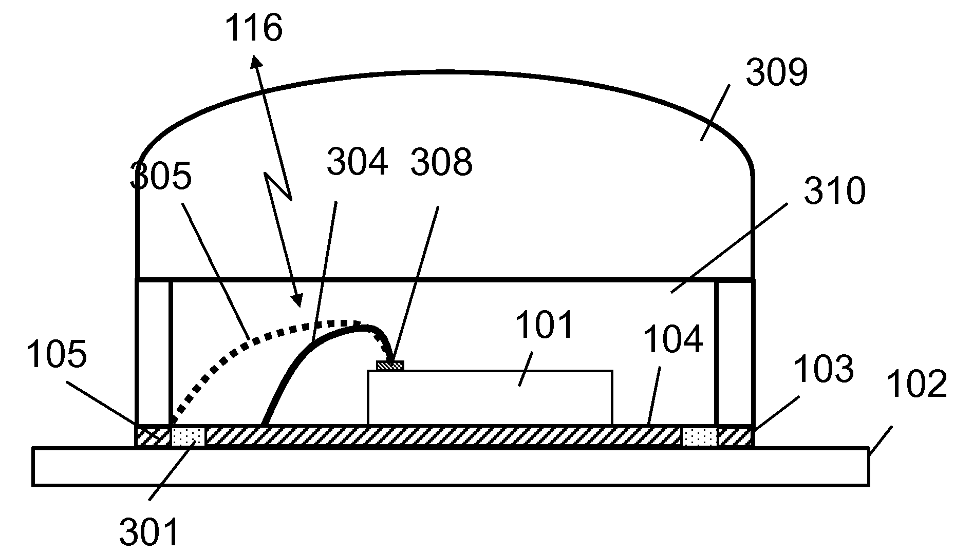
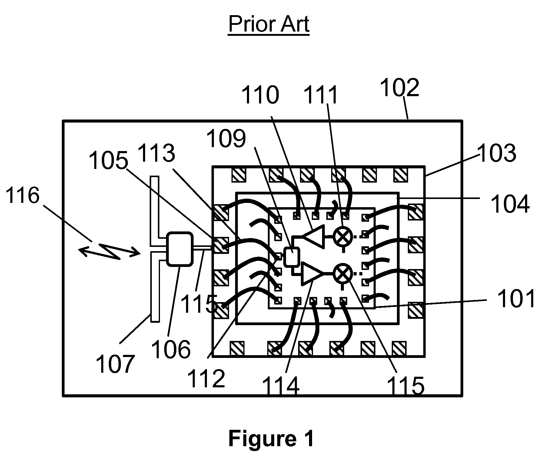
—FIG. 3—ELEVATIONAL VIEW OF PACKAGED IC

[0020]FIG. 3 shows an elevation view of one embodiment, a packaged IC chip. The package is made of an electrically conductive paddle 104, pins 303, and supporting dielectric-material 301. The package contains a chip 101 made of semiconductor material. The package is placed on a PCB 102. The chip constitutes the packaged millimeter-wave transceiver module. The chip contains the transceiver circuit components. The chip is connected to the package by metallic interconnections 304 and 305 that are formed of wires. The interconnections may also be made of, but are not limited to, ribbons, and metallic films. These interconnections are designed as to radiate as an antenna to transmit or receive electromagnetic waves. A dielectric cover 309 may be designed as a dielectric lens. The dielectric cover may be part of package 103. The lens helps change the radiation characteristics of the antenna such as to improve directivity, gain, and coverage.

[0021]In ...


PUM


Abstract

A compact millimeter-wave transmitter and receiver make use of interconnections within a chip-containing package for providing an integrated antenna. Due to shorter wavelength of millimeter-waves, these interconnections can be used as antennas for radiation of electromagnetic waves. A dielectric cover or lens is provided within the package to increase the antenna's directivity and to provide a mechanical shield for the chip.

Description

BACKGROUNDPrior Art[0001]The millimeter-wave radio-frequency band typically spans 30 to 300 GHz. Since RF (radio frequency bands (<10 GHz) are getting crowded by wireless applications, millimeter-wave (mm-wave) bands (>10 GHz) are becoming more popular. In USA, the 60 GHz mm-wave band is unlicensed and has a large usable bandwidth of 7 GHz. It is being proposed for mm-wave short-range high-data-rate systems. Mm-wave wireless systems typically have transmitter and receiver circuitry, collectively called a transceiver. The transceiver is connected to antennas for communicating with another transceiver. The antenna transmits and receives electromagnetic waves through free space, thereby facilitating communication between two different transceivers. Heretofore the art recognized two approaches for implementing a transceiver and antenna combination for the 60 GHz mm-wave band.[0002]The first approach is shown in FIG. 1, which shows a top view of a typical mm-wave module. A semicond...

Claims


Application Information

Patent Timeline
IPC IPC(8): H01Q1/00H01Q9/16
CPCH01L23/66H01L24/48H01L2924/3025H01L2924/01033H01L2924/01023H01L2924/01006H01Q9/16H01Q1/2283H01L2924/3011H01L24/49H01L2223/6611H01L2223/6677H01L2224/056H01L2224/48011H01L2224/48091H01L2224/484H01L2224/49171H01L2224/49175H01L2924/01005H01L2924/01013H01L2924/01029H01L2924/01047H01L2924/01079H01L2924/014H01L2924/14H01L2924/19041H01L2924/30107H01L2924/00014H01L2924/00H01L2924/30111H01L2224/05554H01L2224/023H01L2224/45099H01L2924/00012H01L2924/0001
Inventor RAJANISH, FNUJAIN, NITINMENON, GAURAVALEXANIAN, ANGELOS
Owner ANOKIWAVE
Why Eureka
Try Eureka