

Quantum dot thin film solar cell
a solar cell and quantum dot technology, applied in the direction of electrical equipment, semiconductor devices, capacitors, etc., can solve the problems of increasing the fabrication cost and low energy conversion rate of the solar cell
- Summary
- Abstract
- Description
- Claims
- Application Information
AI Technical Summary
Benefits of technology
Problems solved by technology
Method used
Image

Examples
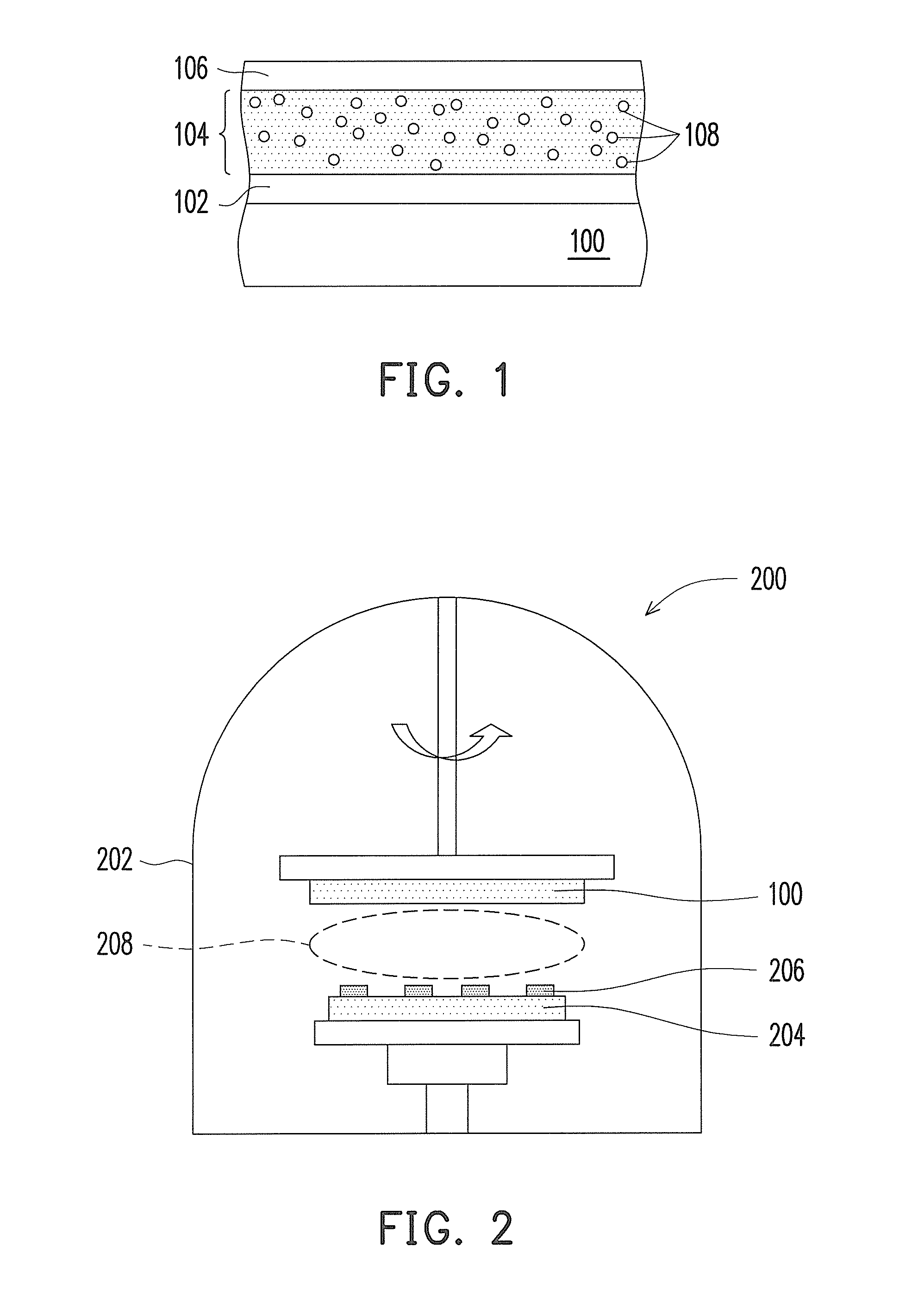
first exemplary embodiment
[0035]FIG. 3 is a structural cross-sectional view of a quantum dot thin film solar cell according to the first exemplary embodiment of the disclosure.
[0036]Referring to FIG. 3, the quantum dot thin film solar cell 300 of the first exemplary embodiment includes a substrate 302, a P-type conductive layer 304, an optical active layer 306, an N-type semiconductor layer 308, and an N-type conductive layer 310, wherein a plurality of quantum dots 312 is formed in the optical active layer 306. Although the quantum dots 312 present an even distribution state in FIG. 3, the disclosure is not limited thereto. In other words, the quantum dots 312 formed in the optical active layer 306 can also present an irregular distribution state.
[0037]Referring to FIG. 3 again, a material of the optical active layer 306 of the first exemplary embodiment is, for example, a substance selected from a substance group consisting of CIGS, CIS, CGS, CGT, and CIAS. For example, if the material of the optical activ...
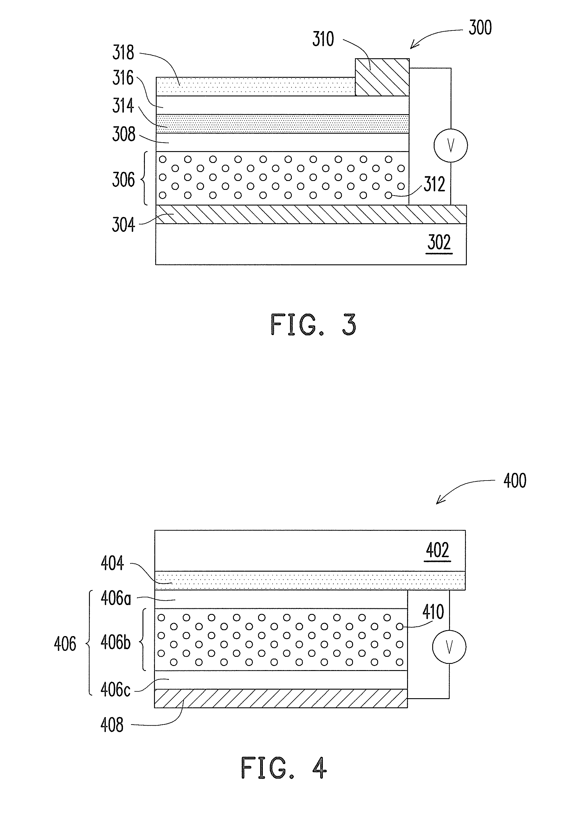
second exemplary embodiment
[0039]FIG. 4 is a structural cross-sectional view of a quantum dot thin film solar cell according to the second exemplary embodiment of the disclosure.
[0040]Referring to FIG. 4, the quantum dot thin film solar cell 400 of the second exemplary embodiment at least includes a substrate 402, a first electrode layer 404 disposed under the substrate 404, a P-i-N silicon thin film layer 406 deposited under the first electrode layer 404, and a second electrode layer 408 disposed under the P-i-N silicon thin film layer 406, wherein a plurality of quantum dots 410 is formed in an intrinsic layer 406b of the P-i-N silicon thin film layer 406. The P-i-N silicon thin film layer 406 is, for example, a structure formed by a-Si, μc-Si or microcrystalline silicon germanium (μc-SiGe). For example, the P-i-N silicon thin film layer 406 may include a P-type hydrogenated amorphous silicon (a-Si:H) layer 406a deposited on the first electrode layer 404, an a-Si:H intrinsic layer 406b deposited on the P-ty...
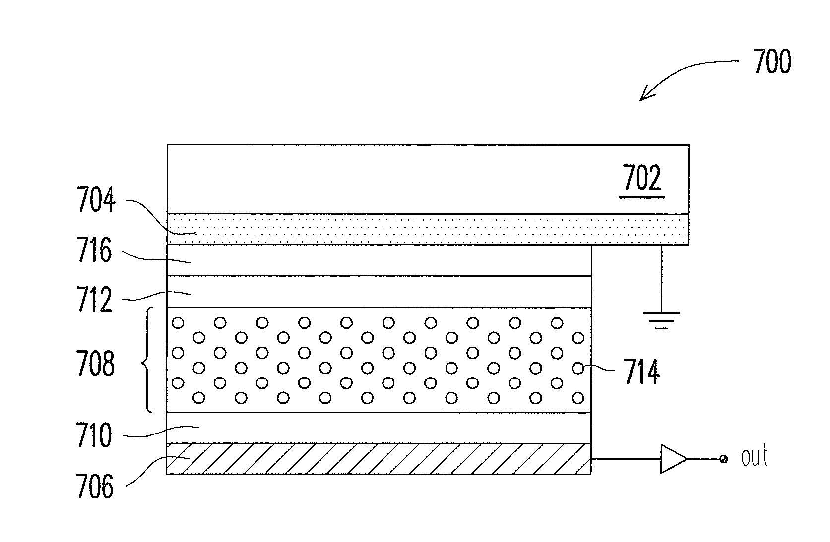
third exemplary embodiment
[0041]FIG. 5 is a structural cross-sectional view of a quantum dot thin film solar cell according to the third exemplary embodiment of the disclosure.
[0042]Referring to FIG. 5, the quantum dot thin film solar cell 500 of the third exemplary embodiment is a tandem solar cell, which at least includes a substrate 502, a first electrode layer 504 disposed on the substrate 502, a P-i-N hyhrogenated microcrystalline silicon (μc-Si:H) thin film formed by an N-type μc-Si:H layer 506a deposited on the first electrode layer 504, a μc-Si:H intrinsic layer 506b and a P-type μc-Si:H layer 506c, a P-i-N a-Si:H thin film foamed by an N-type a-Si:H layer 508a deposited on the P-type μc-Si:H layer 506c, an a-Si:H intrinsic layer 508b and a P-type a-Si:H layer 508c, and a second electrode layer 510 disposed on the P-type a-Si:H layer 508c. In the present exemplary embodiment, quantum dots 514 and 512 are respectively formed in the μc-Si:H intrinsic layer 506b and the a-Si:H intrinsic layer 508b, and ...
PUM
 Abstract
Description
Claims
Application Information