
Silicon dioxide cantilever support and method for silicon etched structures

a technology of silicon dioxide and cantilever support, which is applied in the direction of solid-state devices, capacitors, inductances, etc., can solve the problems of unacceptably large number of device failures, more fragile siosub>2 /sub>membrane, and fragile membrane structures, etc., to reduce parasitic capacitance in an integrated circuit, the effect of robustness and economics

Active Publication Date: 2010-11-18
TEXAS INSTR INC
View PDF1 Cites 30 Cited by
  • Summary
  • Abstract
  • Description
  • Claims
  • Application Information

AI Technical Summary

Benefits of technology

[0023]It is another object of the invention to provide a robust, economical integrated circuit that is operable at higher RF frequencies that have been previously achievable in similar integrated circuits.
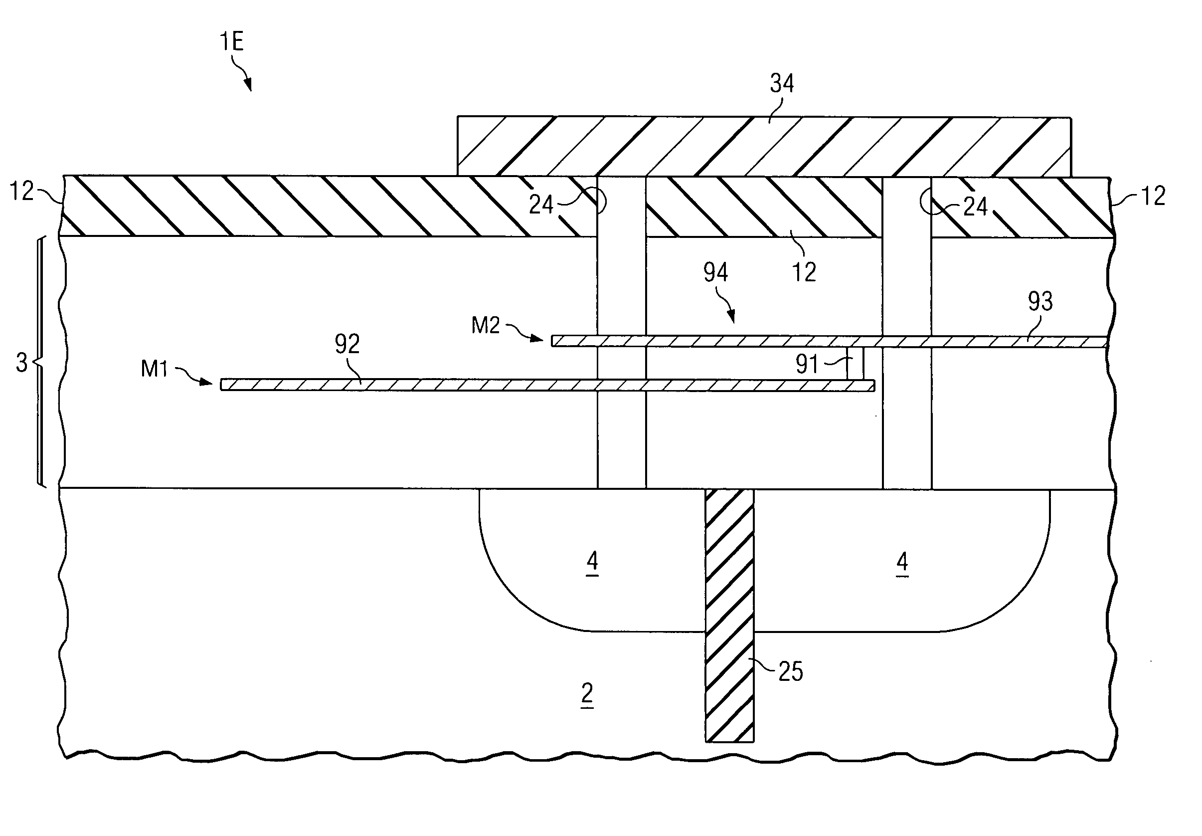
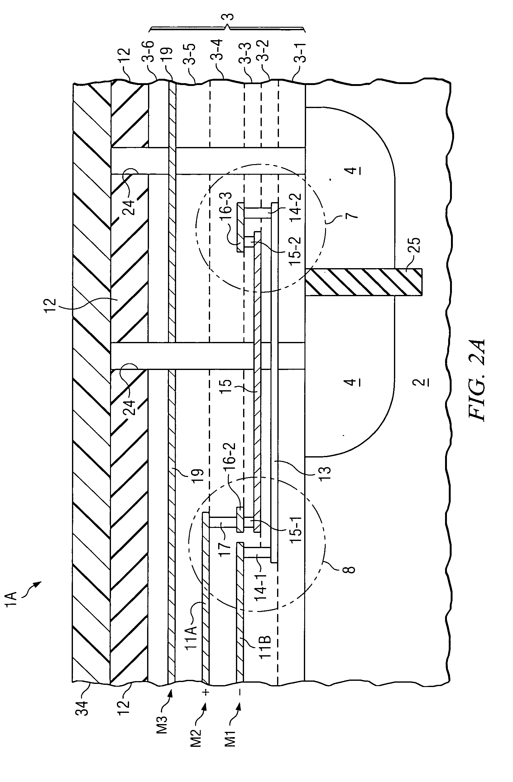
[0031]In one embodiment, the invention provides a method for making a semiconductor device, including forming a deep trench in a semiconductor layer (2), filling the deep trench with SiO2 (25), providing a dielectric layer (3) on the semiconductor layer (2) and the SiO2 (25), forming a plurality of etchant openings (24) through the dielectric layer (3), the etchant openings (24) being proximate to the SiO2 (25), and introducing etchant through the etchant openings (24) to etch a cavity (4) in the semiconductor layer and thereby expose the SiO2 as a SiO2 pillar (25) extending from a bottom of the cavity (4) to engage and support a portion of the dielectric layer (3) extending over the cavity (4), to thereby increase robustness of the semiconductor device. In one embodiment, the method includes providing a cap layer (34) above the dielectric layer (3) to cover the etchant openings (24).

Problems solved by technology

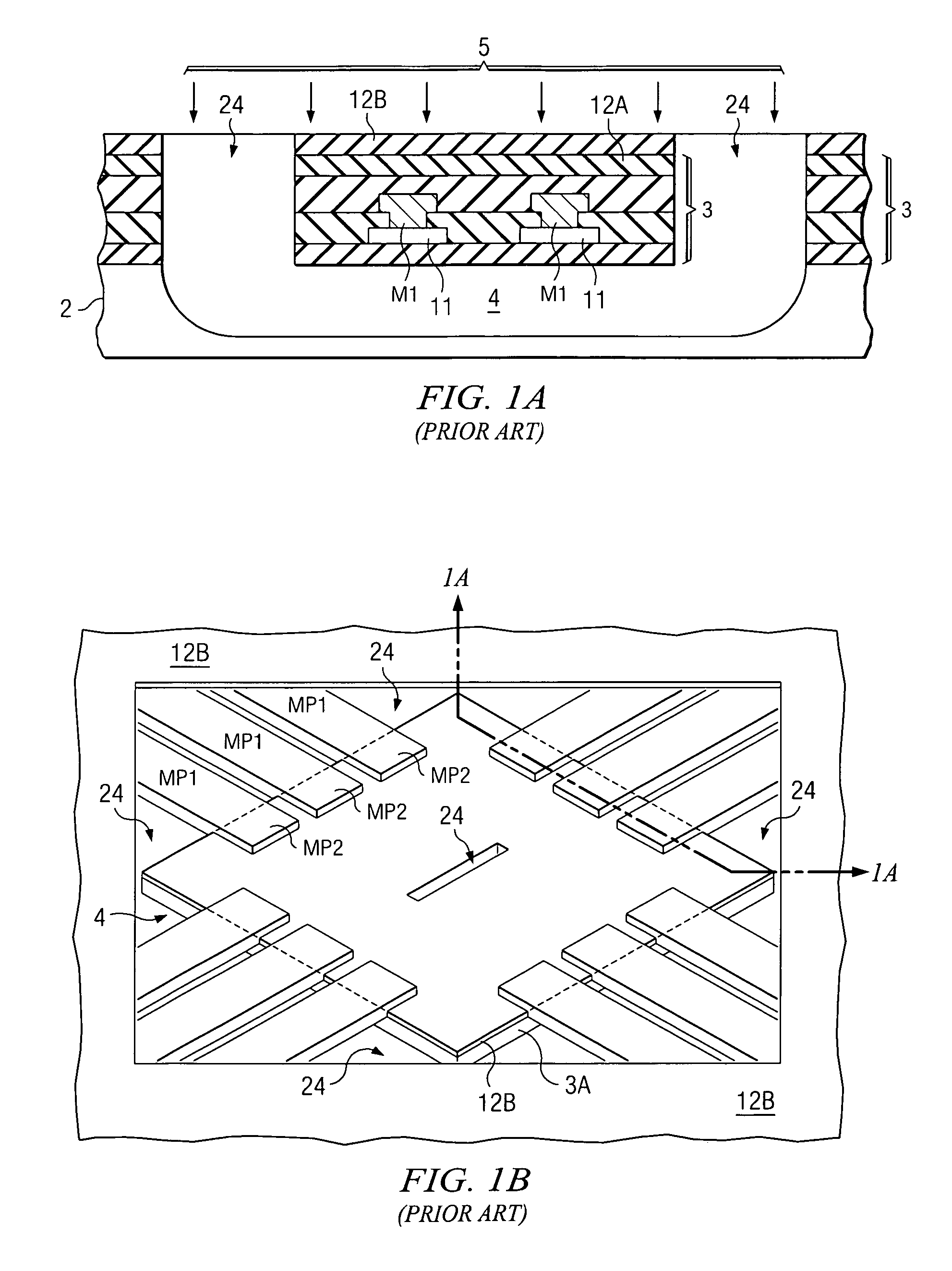
Such membrane structures tend to be fragile and therefore susceptible to damage during assembly operations that occur after formation of the membrane structures.
The larger the cavity opening is, the more fragile the SiO2 membrane will be.
Such fragility ordinarily results in an unacceptably large number of device failures during subsequent wafer fabrication, subsequent packaging, and ultimate utilization of the IR sensor of FIGS. 1A and 1B.

Method used


Image

  • Silicon dioxide cantilever support and method for silicon etched structures
  • Silicon dioxide cantilever support and method for silicon etched structures
  • Silicon dioxide cantilever support and method for silicon etched structures

Examples


Embodiment Construction

[0047]The present invention provides one or more deep trench oxide pillars 25 to act as a support structure under a portion of a subsequently described SiO2 membrane which extends over a subsequently described cavity 4 etched in a silicon layer 2 (FIG. 2A). The deep trench oxide is strong and resistant to the silicon etching process and therefore the oxide pillar is exposed as the cavity is etched into the silicon layer. Ordinary forces on the top surface of the fragile SiO2 membrane therefore will not damage it. Consequently, the present invention makes it more feasible to use standard low cost packaging (WCSP) for the IR sensor disclosed in the above mentioned pending Meinel et al. application. As subsequently explained, the present invention also makes it more feasible to provide greatly reduced parasitic capacitances for resistors and / or capacitors and / or conductors in an integrated circuit.

[0048]FIG. 2A shows a cross-section of an integrated circuit IR sensor chip 1A which incl...


PUM


Abstract

A semiconductor device includes a semiconductor layer (2) having therein a cavity (4). A dielectric layer (3) is formed on the semiconductor layer. A plurality of etchant openings (24) extend through the dielectric layer for passage of etchant for etching the cavity. An SiO2 pillar (25) extends from a bottom of the cavity to engage and support a portion of the dielectric layer extending over the cavity. In one embodiment, a cap layer (34) on the dielectric layer covers the etchant openings.

Description

BACKGROUND OF THE INVENTION[0001]The present invention relates generally to structures and methods for strengthening / supporting dielectric membranes which extend over the over openings / cavities in integrated circuit devices, and more particularly to deep trench oxide post / support structures extending through openings / cavities to support various parts of the membranes.[0002]This invention is related to the structures and methods disclosed in the assignee's pending application “INFRARED SENSOR STRUCTURE AND METHOD” by Walter B. Meinel and Kalin V. Lazarov, Ser. No. 12 / 380,316, filed Feb. 26, 2009, and incorporated herein by reference.[0003]Integrated semiconductor sensors can make use of “cantilevered” silicon dioxide membrane structures which extend from, or “overhang” from, a silicon base or the like. Such membrane structures tend to be fragile and therefore susceptible to damage during assembly operations that occur after formation of the membrane structures. For example, to achiev...

Claims


Application Information

Patent Timeline
Patent Type & Authority Applications(United States)
IPC IPC(8): H01L29/66H01L21/28H01L29/02
CPCH01L21/764H01L27/08H01L28/10H01L28/20H01L28/40H01L31/101
Inventor MEINEL, WALTER B.LAZAROV, KALIN V.GOODLIN, BRIAN E.
Owner TEXAS INSTR INC
Learn More