
Etching cavity structures in silicon under dielectric membrane

a technology of dielectric membrane and cavity structure, which is applied in the direction of optical radiation measurement, instruments, coatings, etc., can solve the problems of unacceptably large number of device failures, unfavorable device maintenance, and fragile membrane structure, etc., to reduce parasitic capacitance in an integrated circuit, the effect of robustness and economics

Active Publication Date: 2015-10-13
TEXAS INSTR INC
View PDF28 Cites 0 Cited by
  • Summary
  • Abstract
  • Description
  • Claims
  • Application Information

AI Technical Summary

Benefits of technology

This approach results in more robust and cost-effective integrated circuits capable of operating at higher RF frequencies with reduced parasitic capacitance, minimizing device failures and stress-induced cracks.

Problems solved by technology

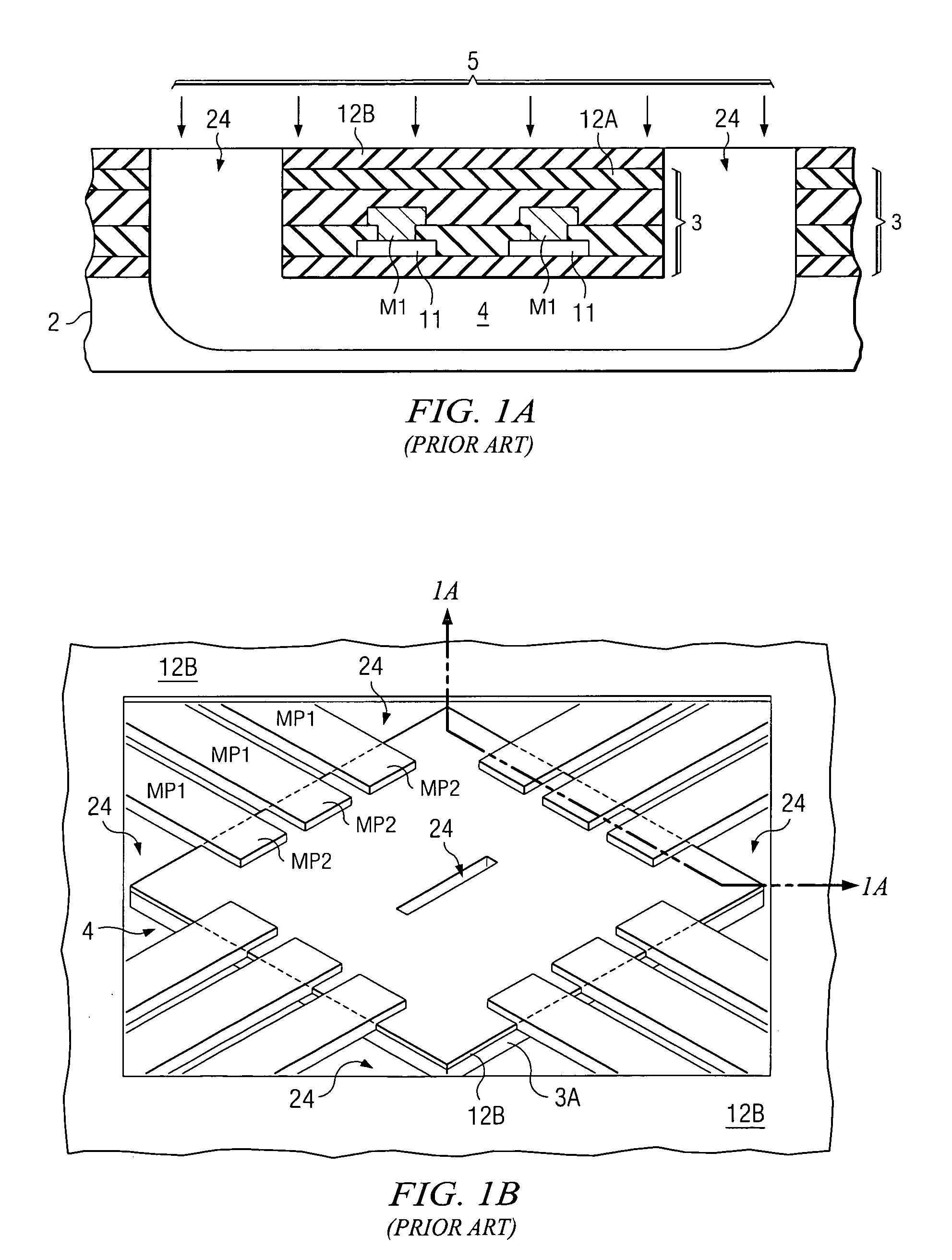
Such membrane structures tend to be fragile and therefore susceptible to damage during assembly operations which occur after formation of the membrane structures.
For example, to achieve maximum sensitivity, the cavity openings covered by the SiO2 membrane in the infrared sensors described in the above mentioned Meinel et al. application should be as large as possible, but unfortunately this causes. the SiO2 membrane to be more fragile.
Such fragility ordinarily results in an unacceptably large number of device failures during subsequent wafer fabrication, subsequent packaging, and ultimate utilization of the IR sensor of FIGS. 1A and 1B.
When performing silicon etching by introducing silicon etchant through openings in a dielectric layer of a semiconductor device wherein the etching undercuts the dielectric layer to provide a cavity underneath the dielectric layer, the resulting undercut dielectric membrane is very fragile and can be damaged during further processing of the semiconductor device.
This causes high stress in the SiO2 membrane over the etched cavity.
Such cracks may result in integrated circuit device failure or unreliable device operation.

Method used


Image

  • Etching cavity structures in silicon under dielectric membrane
  • Etching cavity structures in silicon under dielectric membrane
  • Etching cavity structures in silicon under dielectric membrane

Examples


Embodiment Construction

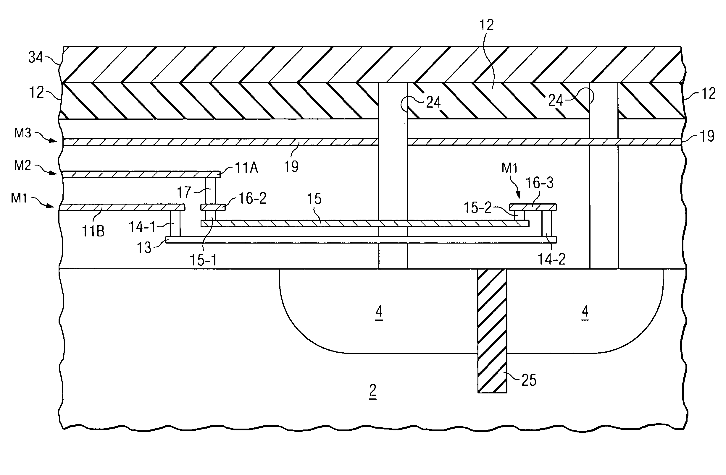
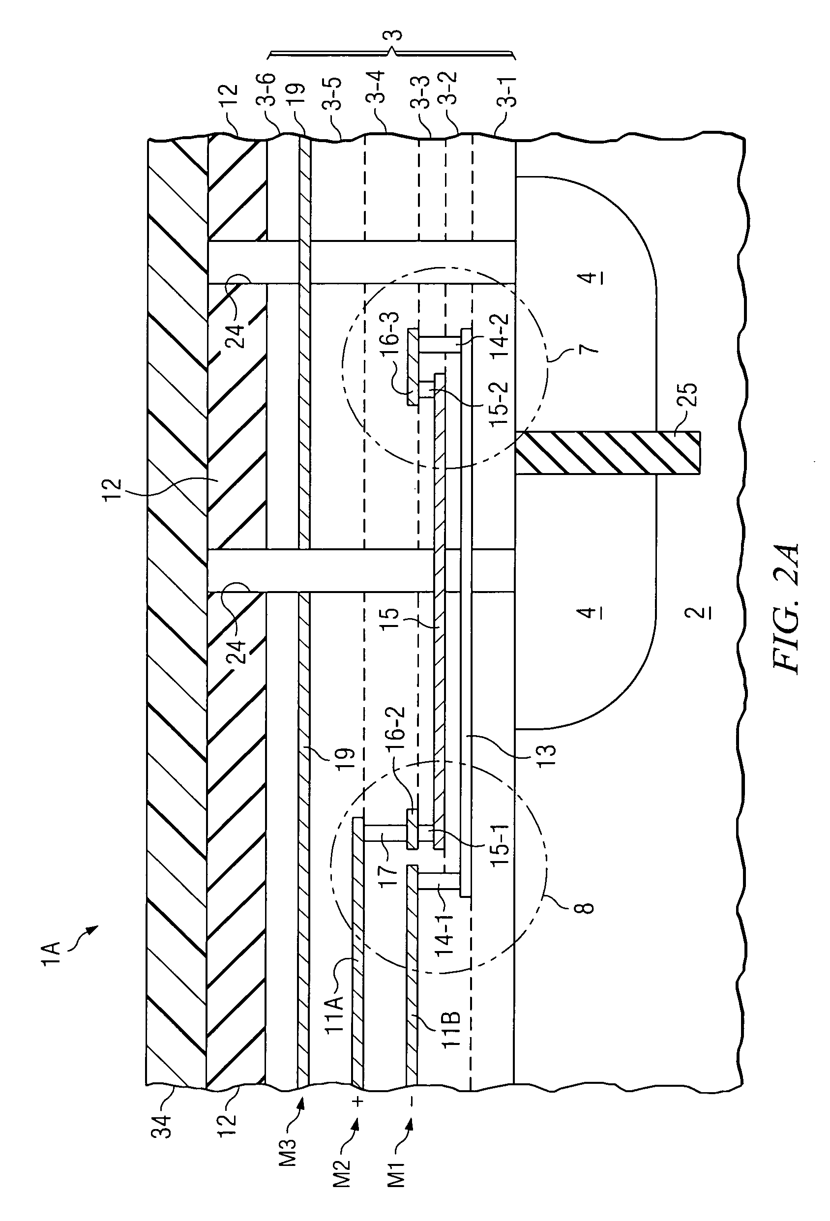
[0056]FIG. 2A shows a cross-section of an integrated circuit IR sensor chip 1A which includes silicon substrate 2 and an etched cavity 4 therein. Silicon substrate 2 in FIG. 2A typically includes a thin layer of epitaxial silicon into which cavity 4 is etched, and also includes the silicon wafer substrate (not shown) on which the epitaxial silicon layer is grown. IR sensor chip 1A includes dielectric stack 3 (also referred to as SiO2 stack 3) formed on the upper surface of silicon layer 2. SiO2 stack 3 includes multiple oxide layers 3-1,2 . . . 6 as required to facilitate fabrication of N-doped polysilicon (polycrystalline silicon) layer 13, titanium nitride layer 15, tungsten contact layers 14-1, 14-2, 15-1, 15-2, and 17, first aluminum metallization layer M1, second aluminum metallization layer M2, third aluminum metallization layer M3, and various elements of CMOS circuitry (not shown), all within SiO2 stack 3.

[0057]The various layers shown in dielectric stack 3, including polysi...


PUM

PropertyMeasurementUnit
diameteraaaaaaaaaa
diameteraaaaaaaaaa
diametersaaaaaaaaaa

Abstract

A semiconductor device includes a semiconductor layer (2) and a dielectric stack (3) on the semiconductor layer. A plurality of etchant openings (24-1,2 . . . ) are formed through the dielectric stack (3) for passage of etchant for etching a plurality of overlapping sub-cavities (4-1,2 . . . ), respectively. The etchant is introduced through the etchant openings to etch a composite cavity (4) in the semiconductor layer by simultaneously etching the plurality of overlapping sub-cavities into the semiconductor layer.

Description

BACKGROUND OF THE INVENTION[0001]The present invention relates generally to structures and methods for strengthening / supporting dielectric membranes which extend over the over cavities in integrated circuit devices, and more particularly to use of various sizes, shapes, and relative locations of etchant openings in the dielectric membranes through which to introduce etchant for etching the cavities.[0002]This invention is closely related to the assignee's pending application “INFRARED SENSOR STRUCTURE AND METHOD” by Walter B. Meinel and Kalin V. Lazarov, Ser. No. 12 / 380,316, filed Feb. 26, 2009, and incorporated herein by reference.[0003]Integrated semiconductor sensors can make use of SiO2 membrane structures which extend from, or “overhang” from, a silicon base or the like, for example, to cover a cavity etched into the silicon base. Such membrane structures tend to be fragile and therefore susceptible to damage during assembly operations which occur after formation of the membran...

Claims


Application Information

Patent Timeline
Patent Type & Authority Patents(United States)
IPC IPC(8): G01J5/12B81C1/00G01J5/02
CPCG01J5/12B81C1/00047G01J5/024G01J5/0225G01J5/02B81B2201/0292
Inventor MEINEL, WALTER B.LAZAROV, KALIN V.GOODLIN, BRIAN E.
Owner TEXAS INSTR INC
Learn More