Solid-state image capture device, manufacturing method therefor, and electronic apparatus

a technology of solid-state image and manufacturing method, which is applied in the direction of radio frequency controlled devices, instruments, television systems, etc., can solve the problems of insufficient improvement in sensitivity, decreased so as to improve manufacturing efficiency, reduce ripple, and improve image quality of captured images

Inactive Publication Date: 2010-11-18
SONY SEMICON SOLUTIONS CORP
View PDF6 Cites 37 Cited by
  • Summary
  • Abstract
  • Description
  • Claims
  • Application Information

AI Technical Summary

Benefits of technology

[0021]According to the present invention, the antireflection layer is formed using a binder resin having a lower refractive index than the on-chip lens and low-refractive-index particles having a lower refractive index than the binder resin. Alternatively, the on-chip lens is formed using a binder resin and low-refractive-index particles having a lower refractive index than the binder resin. Thus, it is possible to reduce ripple due to a phase difference using the curvature of the low-refractive-index particles.
[0022]According to the present invention, it is possible to provide a solid-state image capture device, a manufacturing method therefor, and an electronic apparatus which are capable of improving the image quality of captured images and are capable of improving the manufacturing efficiency.

Problems solved by technology

In the above-described configurations, there are cases in which it is difficult to sufficiently enhance the light focusing efficiency, resulting in an insufficient improvement in the sensitivity.
Consequently, the image quality of captured images may decrease.
There are also cases in which it is difficult to sufficiently suppress generation of flare, ghost, and so on, resulting in a decrease in the image quality of captured images.
However, such an approach may cause problems, such as an increase in complexity in the manufacturing process and an increase in the manufacturing cost.
Thus, there are cases in which it is difficult to improve the image quality of captured images and it is difficult to improve the manufacturing efficiency.

Method used


Image

  • Solid-state image capture device, manufacturing method therefor, and electronic apparatus
  • Solid-state image capture device, manufacturing method therefor, and electronic apparatus
  • Solid-state image capture device, manufacturing method therefor, and electronic apparatus

Examples


first embodiment (

[A] Device Configuration

(1) Configuration of Major Portion of Camera

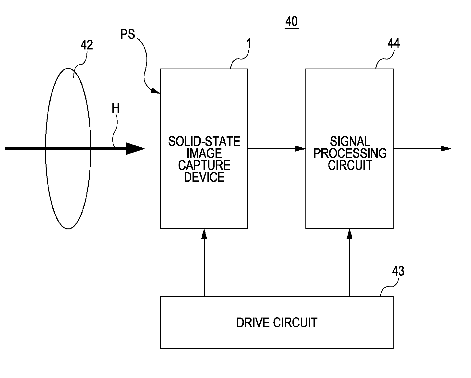
[0050]FIG. 1 is a block diagram showing the configuration of a camera 40 according to a first embodiment of the present invention.

[0051]As shown in FIG. 1, the camera 40 includes a solid-state image capture device 1, an optical system 42, a drive circuit 43, and a signal processing circuit 44. The portions included in the camera 40 are sequentially described below.

[0052]Incident light (of a subject image) H entering through the optical system 42 is received by an image-capture surface PS of the solid-state image capture device 1. The solid-state image capture device 1 then photoelectrically converts the received light to generate signal electric charge. The solid-state image capture device 1 performs driving on the basis of a drive signal output from the drive circuit 43. Specifically, the solid-state image capture device 1 reads the signal electric charge and outputs it as raw data.

[0053]The optical system 42 is di...

second embodiment (

[A] Device Configuration, Etc.

[0153]FIG. 13 is a schematic view showing a major portion of a solid-state image capture device 1b according to a second embodiment of the present invention. FIG. 13 illustrates a cross section of a portion that is similar to the portion shown in FIG. 4.

[0154]As shown in FIG. 13, an on-chip lens 111b of the solid-state image capture device 1b according to the present embodiment is different from the on-chip lens 111 in the first embodiment. An antireflection layer 112b is also different from the antireflection layer 112 in the first embodiment. Except for these points, the present embodiment is the same as the first embodiment. Thus, descriptions of redundant portions are omitted hereinafter.

[0155]As shown in FIG. 13, multiple on-chip lenses 111b are arranged adjacent to each other. More specifically, the multiple on-chip lenses 111b are formed to be integrated with each other without spaces therebetween.

[0156]The antireflection layer 112b is formed so ...

third embodiment (

[A] Device Configuration, Etc.

[0168]FIG. 14 is a schematic view showing a major portion of a solid-state image capture device 1c according to a third embodiment of the present invention. FIG. 14 illustrates a cross section of a portion that is similar to the portion shown in FIG. 4.

[0169]As shown in FIG. 14, an antireflection layer 112c of the solid-state image capture device 1c in the present embodiment is different from the antireflection layer 112 in the second embodiment. Except for this point, the present embodiment is the same as the second embodiment. Thus, descriptions of redundant portions are omitted hereinafter.

[0170]The antireflection layer 112c is formed so as to contain a binder resin (not shown) and low-refractive-index particles (not shown), as in the case of the second embodiment. That is, the antireflection layer 112c is formed so as to contain hollow silica particles.

[0171]In the present embodiment, however, as shown in FIG. 14, the antireflection layer 112c is pr...


PUM

PropertyMeasurementUnit
refractive indexaaaaaaaaaa
particle sizeaaaaaaaaaa
thicknessaaaaaaaaaa

Abstract

A solid-state image capture device includes: at least one photoelectric converter provided at an image capture surface of a substrate to receive incident light at a light-receiving surface of the photoelectric converter and photoelectrically convert the incident light to thereby generate signal charge; at least one on-chip lens provided at the image capture surface of the substrate and above the light-receiving surface of the photoelectric converter to focus the incident light onto the light-receiving surface; and an antireflection layer provided on an upper surface of the on-chip lens at the image capture surface of the substrate. The antireflection layer contains a binder resin having a lower refractive index than the on-chip lens and low-refractive-index particles having a lower refractive index than the binder resin.

Description

BACKGROUND OF THE INVENTION[0001]1. Field of the Invention[0002]The present invention relates to a solid-state image capture device, a manufacturing method therefor, and an electronic apparatus. In particular, the present invention relates to a solid-state image capture device having a photoelectric converter that receives light at a light-receiving surface and photoelectrically converts the received light to thereby generate signal charge, a manufacturing method for the solid-state image capture device, and an electronic apparatus.[0003]2. Description of the Related Art[0004]Electronic apparatuses, such as digital video cameras and digital still cameras, include solid-state image capture devices. Examples of the solid-state image capture devices include CMOS (complementary metal oxide semiconductor) image sensors and CCD (charge coupled device) image sensors.[0005]In the solid-state image capture device, an image capture area having multiple pixels is provided on a surface of a sem...

Claims


Application Information

Patent Timeline
Patent Type & Authority Applications(United States)
IPC IPC(8): H04N5/225H01L31/18G02B1/11G02B1/111H01L27/14H01L27/146H04N5/335H04N5/369H04N5/374
CPCG02B1/11G02B7/02H01L27/1462H01L27/14625H01L27/14627H04N5/2254H01L27/14685H01L31/02161H01L31/0232H01L31/0236H01L33/58H01L27/14645
Inventor OGINO, AKIKOSAYAMA, YUKIHIROSHOYA, TAKAYUKISHIMOJI, MASAYATANAKA, YOSHIKAZU
Owner SONY SEMICON SOLUTIONS CORP
Why Eureka
Try Eureka