Semiconductor structures having both elemental and compound semiconductor devices on a common substrate

a technology of semiconductor devices and semiconductor devices, applied in the field of semiconductor devices, can solve the problems of reducing the output of the device, reducing the isolation of the transistor used in switch-type circuits, and reducing the efficiency of the transistor used in amplifier-type circuits, so as to reduce the negative substrate effect of the device performance, the output conductance of the device is higher, and the output is less.

Active Publication Date: 2010-11-25
RAYTHEON CO
View PDF27 Cites 24 Cited by
  • Summary
  • Abstract
  • Description
  • Claims
  • Application Information

AI Technical Summary

Benefits of technology

[0005]1. Minimize negative substrate effects on the device performance, most notably the substrate conduction that may prevent the complete transistor pinch-off. The lack of pinch-off results in higher device's output conductance that, in turn, leads to lower AC gain, cutoff frequency, power density and drain efficiency in the transistors used in amplifier-type circuits as well as lower isolation in the transistors used in switch-type circuits.

Problems solved by technology

Because a CS epitaxial structure needs to be grown on top of the seed layer whose crystal structure and electronic properties are different from those of the CS layer, the CS device performance may deteriorate very significantly due to the formation of an unwanted interface layer between seed and CS layers.
1. Minimize negative substrate effects on the device performance, most notably the substrate conduction that may prevent the complete transistor pinch-off. The lack of pinch-off results in higher device's output conductance that, in turn, leads to lower AC gain, cutoff frequency, power density and drain efficiency in the transistors used in amplifier-type circuits as well as lower isolation in the transistors used in switch-type circuits.
2. Allow for low series resistance, loss series inductance and low shunt capacitance interconnect between the individual heterogeneously integrated individual CS and silicon CMOS FETs.

Method used


Image

  • Semiconductor structures having both elemental and compound semiconductor devices on a common substrate
  • Semiconductor structures having both elemental and compound semiconductor devices on a common substrate
  • Semiconductor structures having both elemental and compound semiconductor devices on a common substrate

Examples


Embodiment Construction

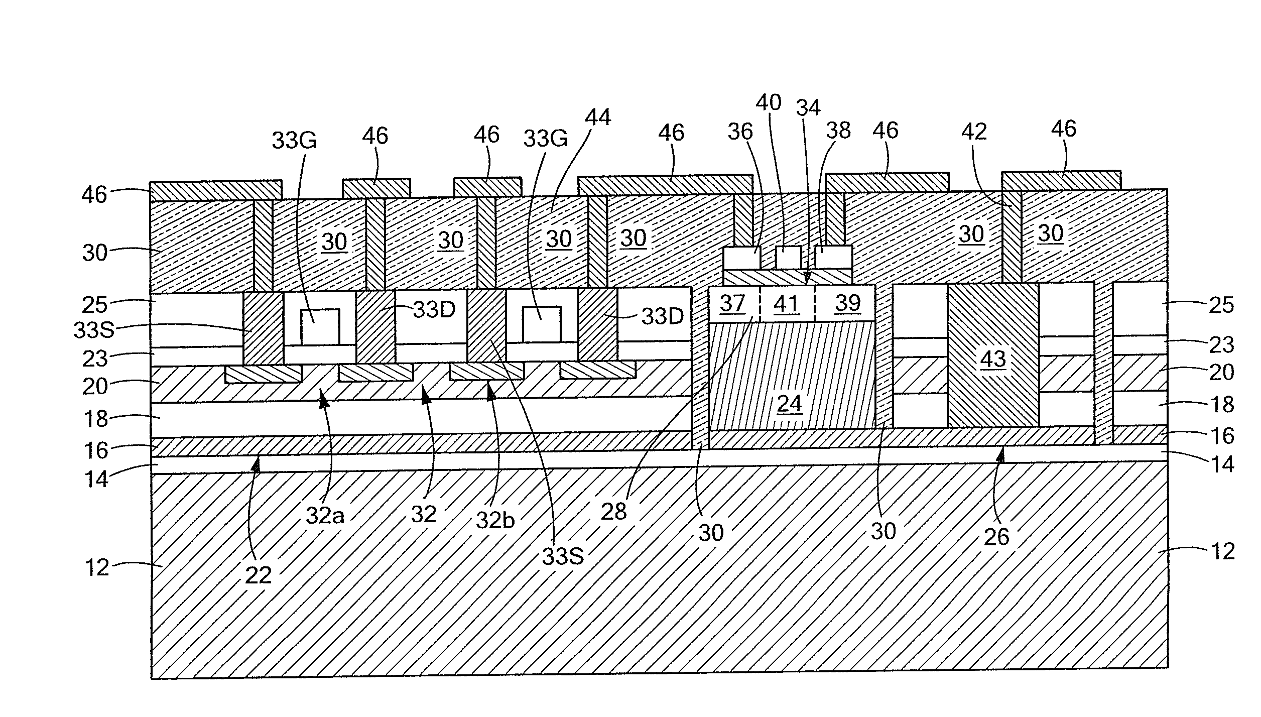
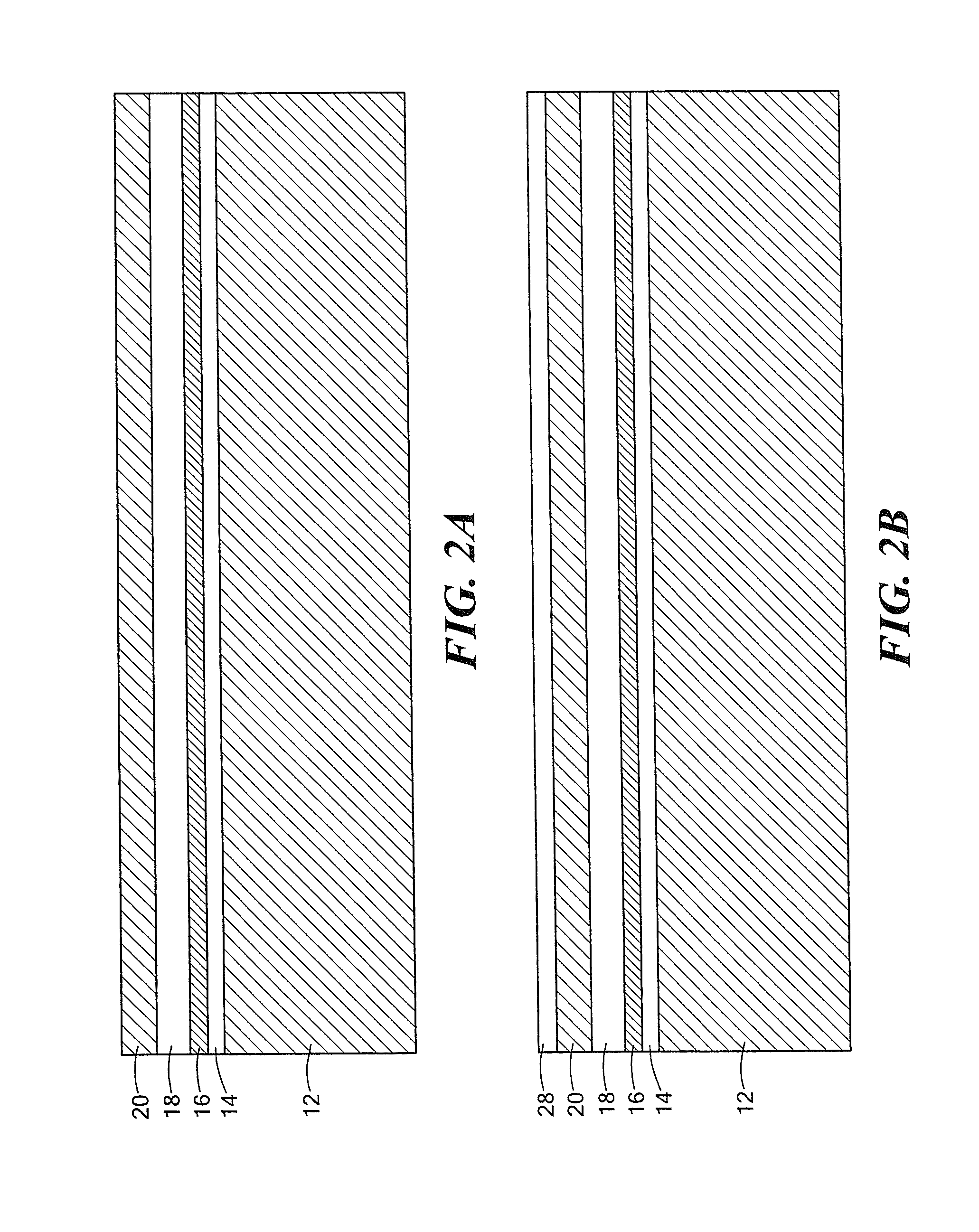
[0023]Referring now to FIG. 1, a semiconductor structure 10 is shown comprising: a substrate 12, here silicon; an insulating layer 14, here silicon dioxide, on the substrate 12; a seed layer 16, here germanium, on the insulating layer 14 and hence supported by the substrate 12; a second insulating layer 18, here silicon dioxide, on the seed layer 16; an elemental semiconductor layer 20, here silicon, disposed over a first portion 22, of the seed layer 16; and a compound semiconductor layer, here III-V material, such as, for example, GaAs or InP, buffer layer 24 disposed on a second portion 26 of the seed layer 16 and an active layer 28, here the same compound semiconductor material as layer 24. The first portion 22 of the seed layer 16 is electrically insulated from the second portion 26 of the seed layer 16 by an insulating material, 30, here for example, Benzocyclobutene (BCB).

[0024]At least one first semiconductor device, here a pair CMOS transistors 32, transistor 32a and 32b, i...


PUM


Abstract

A semiconductor structure comprising: a substrate; a seed layer supported by the substrate; an elemental semiconductor layer disposed over a first portion of the seed layer; and a compound semiconductor layer disposed on a second portion of the seed layer. The first portion of the seed layer is electrically insulated from the second portion of the seed layer. A first semiconductor device is formed in the elemental semiconductor layer. A second semiconductor device is formed in the compound semiconductor layer. The second semiconductor device includes: a first electrode in contact with a first region of the compound semiconductor layer; a second electrode in contact with a second region of the compound semiconductor layer; and a third electrode. The third electrode controls carriers passing in a third region of the compound semiconductor layer disposed between the first region and the second region. A fourth electrode is in electrical contact with the second portion of the seed layer.

Description

TECHNICAL FIELD[0001]This invention relates generally to semiconductor structures and more particularly having both elemental semiconductor devices and compound semiconductor devices on a common substrate.BACKGROUND AND SUMMARY[0002]As is known in the art, with the recent advances enable growth of both compound semiconductor (CS) devices, such as for example III-V FETS or opto-electric devices, and elemental semiconductor (ES) devices, such as for example CMOS devices on a common, such as a silicon, substrate. Thus, the term “compound semiconductor” usually refers to any non-homogeneous semiconductor layers (GaAs, InP, GaN, InSb, AlGaAs, AlGaN, . . . ) as opposed to “elemental semiconductors” (Si, Ge, . . . ). Compound semiconductors can be combination of two or more elements of the periodic table from columns III and V (GaAs, GaN, InP, AlGaAs, . . . ); II and VI (ZnO, CdSe, . . . ); IV-IV (SiGe, SiC), etc. The growth of both compound semiconductor (CS) devices and elemental semicon...

Claims


Application Information

Patent Timeline
Patent Type & Authority Applications(United States)
IPC IPC(8): H01L29/78
CPCH01L21/8258H01L27/0605H01L29/78H01L29/12H01L27/1203
Inventor KAPER, VALERY S.BETTENCOURT, JOHN P.LAROCHE, JEFFREY R.TABATABAIE, KAMAL
Owner RAYTHEON CO
Why Eureka
Try Eureka