
Field Device Having an Analog Output

a field device and output technology, applied in the field of measuring transducers, can solve the problems of high electric power consumption, high cost, and limited available energy, and achieve the effect of reducing power consumption and achieving greater dynamic rang

Inactive Publication Date: 2010-12-02
SIEMENS AG
View PDF13 Cites 9 Cited by
  • Summary
  • Abstract
  • Description
  • Claims
  • Application Information

AI Technical Summary

Benefits of technology

[0008]It is therefore an object of the invention to provide a field device having an analog output, i.e., a measuring transducer for process instrumentation having a 4-20 mA interface as the analog output, which has a low power consumption and by which a high-resolution analog output signal having a greater dynamic range can be generated.
[0010]In accordance with the invention, each stage handles a part of the resolution. Consequently, substantially higher dynamics can be achieved when a microcontroller is used to generate the time signals for the pulse width modulation at the same clock rate. On the other hand, the microcontroller can now be clocked at a lower frequency to achieve predefined dynamics, with the result that the energy consumption of the microcontroller drops and consequently more energy is available for the actual measurement function of a measuring transducer. This can be used to improve the measurement accuracy of the measuring transducer.
[0011]A microcontroller is already present in the majority of field devices. As a result, a particularly simple implementation of the digital / analog converter can be achieved if the digital / analog converter is suitably programmed to split the digital value into a digital coarse portion and a digital fine portion and generates the time signals required for controlling the pulse width modulators.
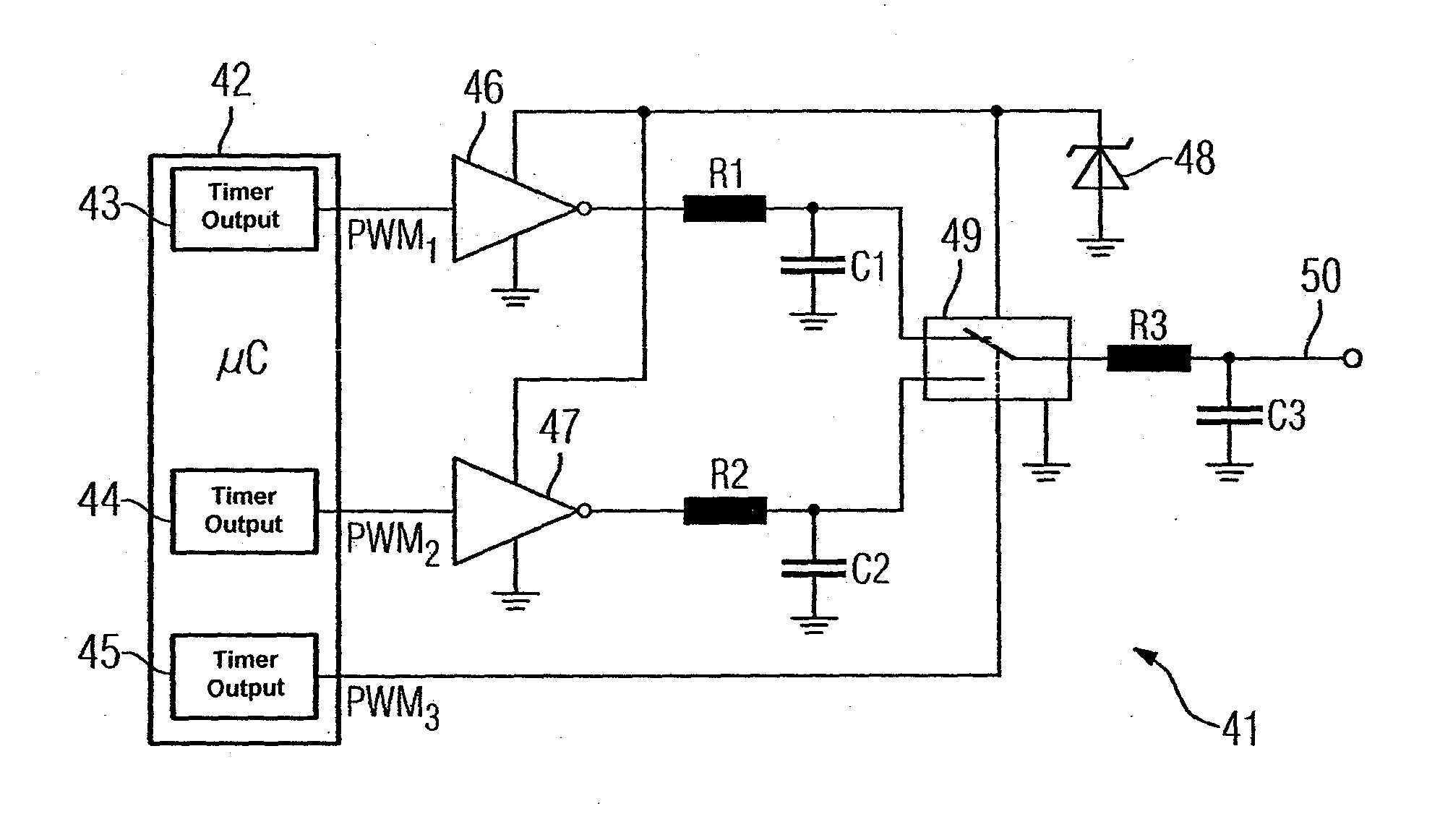
[0012]A particularly high level of precision of the digital / analog conversion is advantageously possible if the low-pass filters of the digital / analog converter are implemented using passive components and are dimensioned such that their input resistance is substantially higher in comparison to the output resistance of the pulse width modulators.
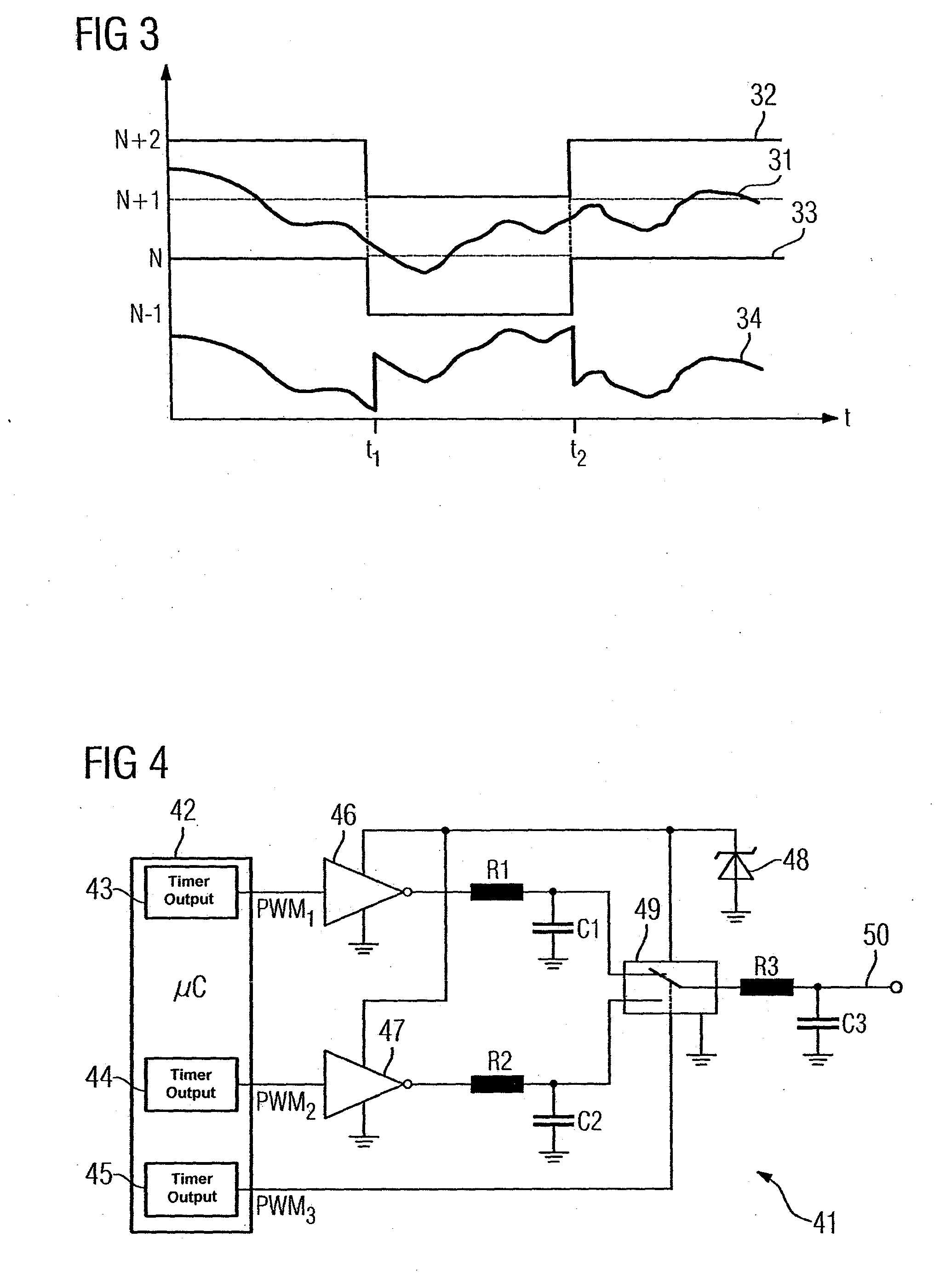
[0013]In order to ensure that poor dynamics of one stage do not have an unfavorable effect on the overall dynamics of the digital / analog conversion, the dynamics of the stages should optimally be identical. This can be achieved in a simple manner if the resolution of the coarse portion and the resolution of the fine portion correspond to the same number of bits. This means that the digital coarse portion essentially corresponds to the N most significant bits and the digital fine portion essentially corresponds to the m least significant bits of the digital value and N is approximately equal to m. Noise in the analog output signal can largely be avoided if the coarse portion is generated using hysteresis.

Problems solved by technology

What is disadvantageous with components of this type, however, are the costs associated therewith, as well as their high electric power consumption.
In particular, in cases where field devices are supplied with the energy required for their operation via a 4-20 mA interface, a significant disadvantage is created because the available energy is very limited.
However, this arrangement is problematic in that a compromise must be made between the achievable dynamics and the adjustment precision of the analog signal, because the frequency of the pulse-width-modulated signal, which frequency has a direct impact on the dynamics, results from the bit resolution of the digital / analog conversion and the clock rate of the microcontroller and is proportional to the product of these two variables.
The clocking of the microcontroller has a direct effect on its power consumption and cannot be increased at will.
On the other hand, the frequency of the pulse-width-modulated signal cannot be arbitrarily reduced in order to achieve a higher bit resolution, because this is a determinant factor in the dynamics of the generated analog output signal.

Method used


Image

  • Field Device Having an Analog Output
  • Field Device Having an Analog Output
  • Field Device Having an Analog Output

Examples


Embodiment Construction

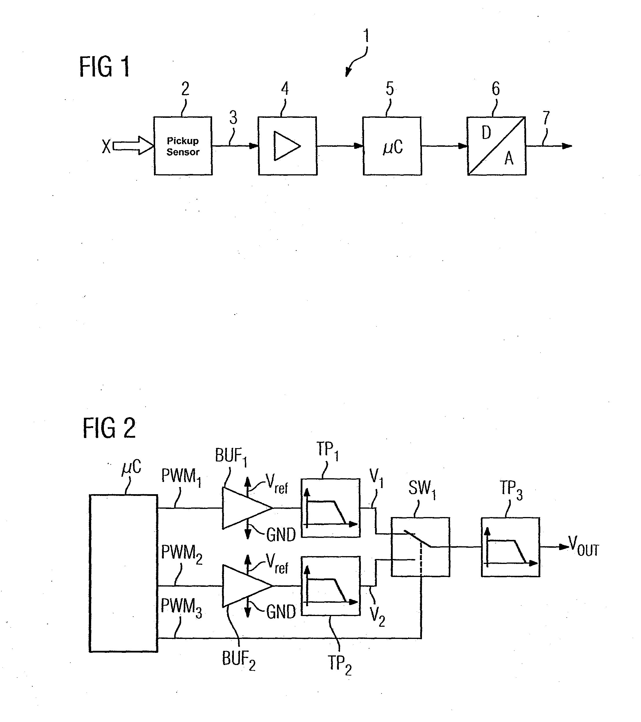
[0020]With reference to FIG. 1, a measuring transducer 1 for measuring a physical or chemical variable X of a process has a pickup sensor 2 which converts the variable into a measurement signal 3. The measurement signal 3 is amplified and digitized in a preprocessing stage 4. The measurement signal preprocessed in this way is supplied in digital form to a microcontroller 5 which, for example, compensates for non-linearities and temperature effects and calculates the measured value to be output. The digital measured value calculated in the microcontroller 5 is converted in a digital / analog converter 6 into an analog output signal which is output via a 4-20 mA interface 7 for further use in a process engineering plant in which the measuring transducer 1 is used.

[0021]For purposes of digital / analog conversion, a microcontroller μC shown in FIG. 2 generates three time signals PWM1, PWM2 and PWM3. The time signals PWM1 and PWM2 are determined in accordance with a coarse portion of the di...


PUM


Abstract

A field device having an analog output, i.e., a measuring transducer, for process instrumentation having a 4-20 mA interface as the analog output. For digital-to-analog conversion, a digital value is split into a digital coarse portion and a digital fine portion. Depending on the digital coarse portion, a first analog signal is generated using a pulse width modulator having a downstream mounted low path filter and a signal above the analog output signal, and a second output signal using a pulse width modulator also having a downstream mounted low path filter with a signal below the analog output signal. The analog signals are supplied to a third pulse width modulator controlled with the digital fine portion, where a low-pass filter (TP3) is downstream mounted. As a result, an analog output signal is provided having a high resolution and good dynamic properties. In addition, the field device is provided with a digital-to-analog converter that can be produced having minimal complexity.

Description

CROSS-REFERENCE TO RELATED APPLICATIONS[0001]This is a U.S. national stage of International Application No. PCT / EP2008 / 062946, filed on 26 Sep. 2008. Priority is claimed on German Application No. 10 2007 046 560.4, filed on 28 Sep. 2007.BACKGROUND OF THE INVENTION[0002]1. Field of the Invention[0003]The invention relates to a field device having an analog output, and, more particularly, to a measuring transducer for process instrumentation having a 4-20 mA interface as the analog output.[0004]2. Description of the Related Art[0005]DE 199 30 661 A1 discloses field devices having analog outputs. In process instrumentation, measuring transducers having a 4-20 mA interface are used in a multiplicity of applications for measuring physical or chemical variables, such as pressure, temperature or a pH value. The transducers typically have a sensor whose sensor signal is amplified, digitized, and subsequently analyzed in a microcontroller to correct the linearity and temperature characterist...

Claims


Application Information

Patent Timeline
IPC IPC(8): H03M1/66
CPCG01D3/024H03M1/822H03M1/68
Inventor CHEMISKY, ERICGEPPERT, MICHAELHAHN, ULRICHROHRBACH, SIMON
Owner SIEMENS AG
Learn More