

Semiconductor storage device, method of controlling the same, and error correction system
a technology of semiconductor storage devices and error correction systems, applied in the direction of coding, instruments, code conversion, etc., can solve the problems of large circuit scale, high error correction capability of mechanisms, and increase in probability of occurrence of errors
- Summary
- Abstract
- Description
- Claims
- Application Information
AI Technical Summary
Benefits of technology
Problems solved by technology
Method used
Image

Examples
first embodiment
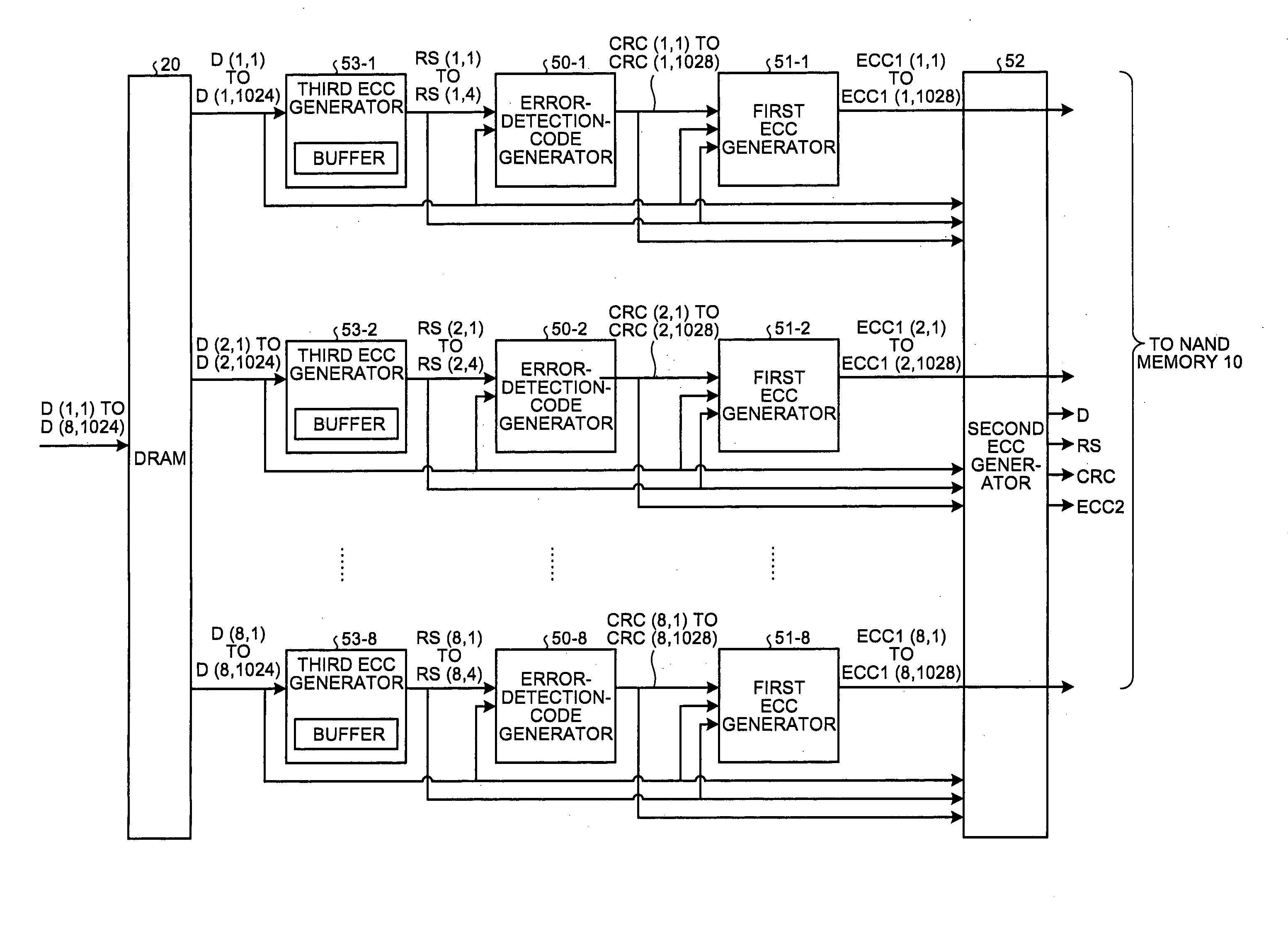
[0034]the present invention allows reduction of a power consumption and a circuit scale by performing three types of correction coding with different error correction capabilities when error correction coding / decoding is applied to a memory such as a flash memory having a defective bit.
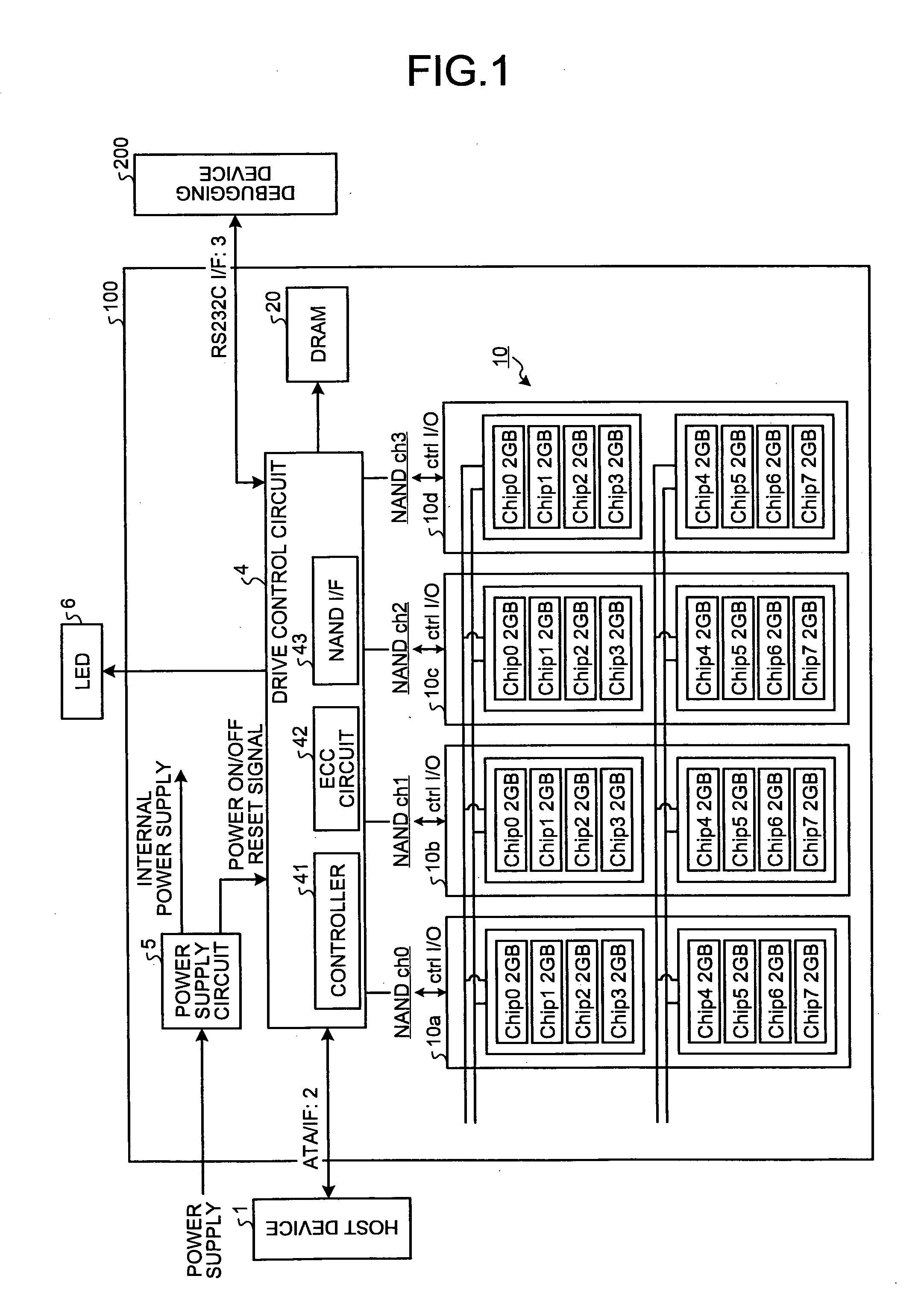
[0035]FIG. 1 is a block diagram of a configuration example of a solid state drive (SSD) 100. The SSD 100 is connected to a host device (host) 1 such as a personal computer or a central processing unit (CPU) core via a memory-connection interface such as an advanced technology attachment (ATA) interface (I / F) (ATA / IF) 2, so that the SSD 100 functions as an external memory of the host device 1. The SSD 100 can perform data transmission / reception with a debugging device 200 via a communication interface 3 such as an RS232C interface (RS232C I / F). The SSD 100 includes a NAND flash memory (hereinafter, “NAND memory”) 10 being a nonvolatile memory, a drive control circuit 4 being a controller, a dynamic ran...
second embodiment
[0129]FIG. 22 is a block diagram of a main portion of a decoding system in an ECC circuit 242 according to the The decoding system of the ECC circuit 242 does not need to incorporate the third ECC correcting unit, and thus, the circuit scale can be reduced.
[0130]According to the second embodiment, because the third error correction is performed by the host device 201, there is no need to perform the third error correction by the SSD 100, which allows reduction in the load on the SSD 100 and in the circuit scale.
[0131]In the second embodiment, the present invention is applied to the SSD having the NAND memory, however, the present invention may be applied to any SSD having other flash electrically erasable programmable read-only memory (EEPROM) such as an NOR type memory.
PUM
 Abstract
Description
Claims
Application Information