Substrate processing apparatus and manufacturing method of semiconductor device

Active Publication Date: 2010-12-16
KOKUSA ELECTRIC CO LTD
View PDF0 Cites 8 Cited by
  • Summary
  • Abstract
  • Description
  • Claims
  • Application Information

AI Technical Summary

Benefits of technology

[0023]According to, the substrate processing apparatus and the manufacturing method of the semiconductor device according to the present invention, residual amounts of chlorine atoms and oxygen atoms in a metal

Problems solved by technology

However, for example, when the high heat treatment is applied to the titanium nitride film formed as an upper electrode and a lower electrode of a capacitor of DRAM, characteristics of a capacitor insulating film sandwiched between titanium nitride films is deteriorated and a leak current is increased in some cases.
Further, diffusion occurs in a source region and a drain region which are previously formed in the substrate, thus deteriorating the circuit characteristics and reducing a performance of a semiconductor device in some cases.
Meanwhile, when the c

Method used


Image

  • Substrate processing apparatus and manufacturing method of semiconductor device
  • Substrate processing apparatus and manufacturing method of semiconductor device
  • Substrate processing apparatus and manufacturing method of semiconductor device

Examples


Embodiment Construction

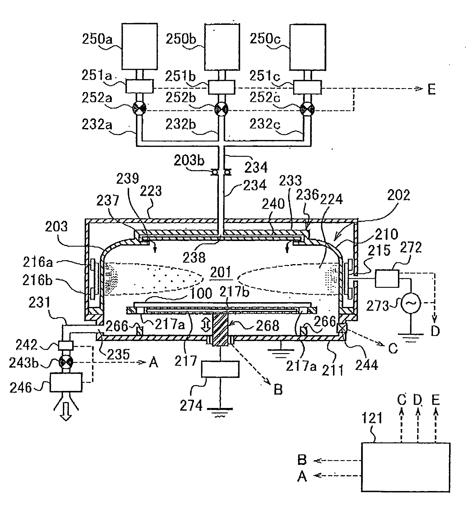
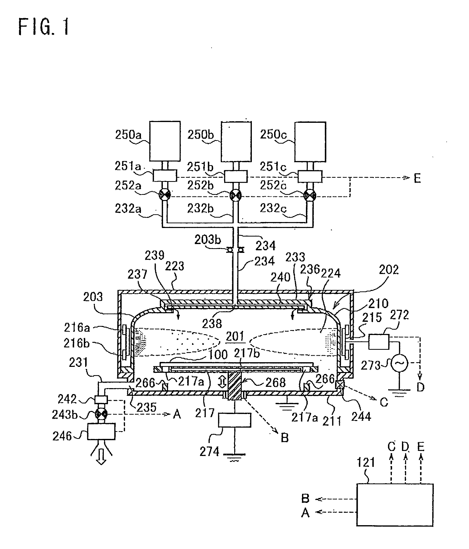
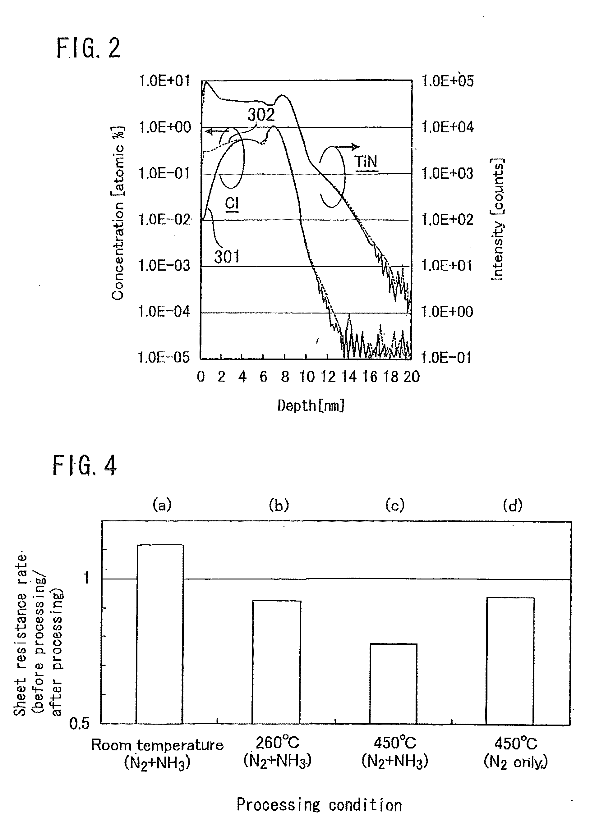
[0030]As described above, when high heat treatment is applied to a titanium nitride film at for example 750° C. or more, the characteristics of other film adjacent to the titanium nitride film are deteriorated, thus increasing a leak current of a capacitor of DRAM in some cases. Further, diffusion occurs in a source region and a drain region which are previously formed in a substrate, thus deteriorating circuit characteristics and reducing performance of a semiconductor device in some cases. Meanwhile, when chlorine atoms are removed in a temperature range of not deteriorating the characteristics of the film adjacent to the titanium nitride film, it is difficult to sufficiently remove residual chlorine.

[0031]Therefore, inventors of the present invention performs strenuous efforts regarding a method of reducing residual amounts of chlorine and oxygen in a titanium nitride film and improving oxidation resistance of the titanium nitride film, in a temperature range of not deteriorating...


PUM

PropertyMeasurementUnit
Plasma poweraaaaaaaaaa

Abstract

To reduce a residual amount of chlorine atoms and oxygen atoms in a metal nitride film, and improve oxidation resistance of the metal nitride, film, in a temperature range of not deteriorating the characteristics of other film adjacent to the metal nitride film. A substrate processing apparatus is provided, comprising: a processing chamber into which a substrate is loaded, having thereon a substrate containing oxygen atoms, chlorine atoms, and metal atoms; a substrate support part for supporting and heating the substrate in the processing chamber; a gas supply part for supplying nitrogen atoms-containing gas and hydrogen atoms-containing gas into the processing chamber; a gas exhaust part for exhausting inside of the processing chamber; a plasma generation part for exciting the nitrogen atoms-containing gas and the hydrogen atoms-containing gas supplied into the processing chamber; and a control part for controlling the substrate support part, the gas supply part, and the plasma generation part.

Description

BACKGROUND OF THE INVENTION[0001]1. Field of the Invention[0002]The present invention relates to a substrate processing apparatus for processing a substrate by using plasma and a manufacturing method of a semiconductor device.[0003]2. Description of the Related Art[0004]In a semiconductor logic device and a DRAM device, etc, for example, a metal nitride film (simply called a titanium nitride (TiN) film hereafter) containing titanium nitride is used as materials of an electrode and wiring, etc, for inhibiting an increase of an electric resistance associated with microfabrication of the device. The metal nitride film can be formed by, for example, Chemical Vapor Deposition (CVD) and Atomic Layer Deposition (ALD). Titanium tetrachloride (TiCl4) gas containing chlorine is used as a precursor gas, to form the titanium nitride film by such methods. For example, patent document 1 describes a method of forming the titanium nitride film.[0005](Patent document 1) WO / 2007 / 020874 Pamphlet[0006]...

Claims


Application Information

Patent Timeline
IPC IPC(8): H01L21/46
CPCC23C16/34C23C16/56H01J37/3244H01L28/60H01J2237/2001H01L21/76856H01L21/76862H01J37/32449
Inventor HORIE, TADASHIHIRANO, AKITOTERASAKI, TADASHI
Owner KOKUSA ELECTRIC CO LTD
Why Eureka
Try Eureka