Method and circuit implementation for reducing the parameter fluctuations in integrated circuits

a technology of integrated circuits and parameter fluctuations, which is applied in the field of method and circuit implementation for reducing the effects of process, supply voltage and temperature variations in integrated circuits, can solve the problems of significant challenges in low-voltage analog circuit design, performance degradation or even malfunction of its application circuits, and achieve the effects of reducing process effects, increasing circuit complexity and power consumption, and reducing supply voltag

Inactive Publication Date: 2010-12-23
LUO HAO +3
View PDF23 Cites 10 Cited by
  • Summary
  • Abstract
  • Description
  • Claims
  • Application Information

AI Technical Summary

Benefits of technology

[0011]Therefore, there is a need in the art to provide a method and circuit implementation that reduces the effects of process, supply voltage and temperature variations in analog ICs, especially in sub-threshold ICs, without significantly increasing the circuit complexity and power consumption.
[0012]Because of the technical difficulties between the present invention and the cited references, it is absolutely not obvious for a person with ordinary skills in the art to utilize the prior arts to come out the solutions disclosed in the present invention.
[0013]The object of the invention is to overcome at least some of the drawbacks relating to the compromise designs of prior art systems and methods as discussed above.
[0014]An object of the present invention is to provide a method for reducing the effects of process, supply voltage and temperature variations in ICs to solve the above-described problem. Another object of the present invention is to provide a body-modulated circuit for realizing the method above. A third object of the present invention is to provide an application of the body-modulated circuit to ICs, especially sub-threshold ICs, realizing a body-modulated class-C inverter circuit, an inverter-based integrator circuit and an inverter-based ΣΔ (Sigma-Delta) modulator circuit with low process-related, supply-voltage-related and temperature-related sensitivity, high stability and strong practicability as compared with the related prior arts.
[0015]According to the first aspect of the present invention, there is provided a method for reducing the effects of process, supply voltage and temperature variations in ICs including the following steps: an induction MOS transistor f

Problems solved by technology

The rapid development of portable electronic device market is forcing an explosive growth in the demand for low-voltage micro-power integrated circuits (ICs).
However, to avoid leakage current in transistors, the threshold voltage is not scaled as aggressively as the supply voltage with continuing scaling of CMOS technology, which poses significant challenges in low-voltage analog circuit design.
However, for a MOS transistor in a sub-threshold region, its parameters, such as transconductance and drain-source current, significantly fluctuate depending upon process, supply voltage and temperature variations, resulting in performance degradation or even malfunction of its application circuits, which disadvantageously affects the stability, reliability and product yield

Method used


Image

  • Method and circuit implementation for reducing the parameter fluctuations in integrated circuits
  • Method and circuit implementation for reducing the parameter fluctuations in integrated circuits
  • Method and circuit implementation for reducing the parameter fluctuations in integrated circuits

Examples


Embodiment Construction

[0041]The present inventions now will be described more fully hereinafter with reference to the accompanying drawings, in which some examples of the embodiments of the inventions are shown. Indeed, these inventions may be embodied in many different forms and should not be construed as limited to the embodiments set forth herein; rather, these embodiments are provided by way of example so that this disclosure will satisfy applicable legal requirements. Like numbers refer to like elements throughout.

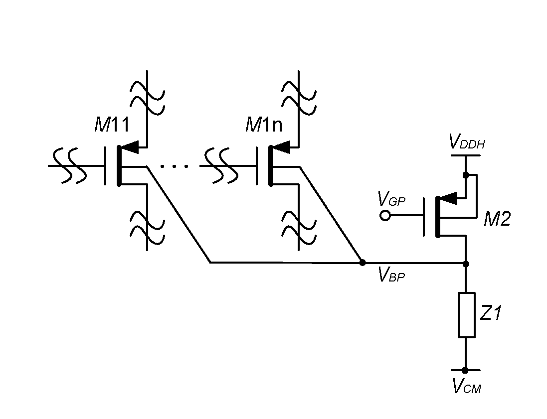
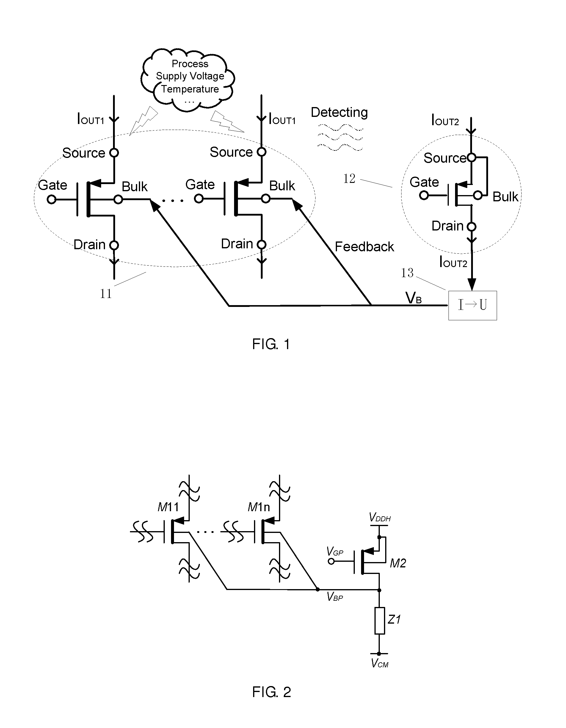
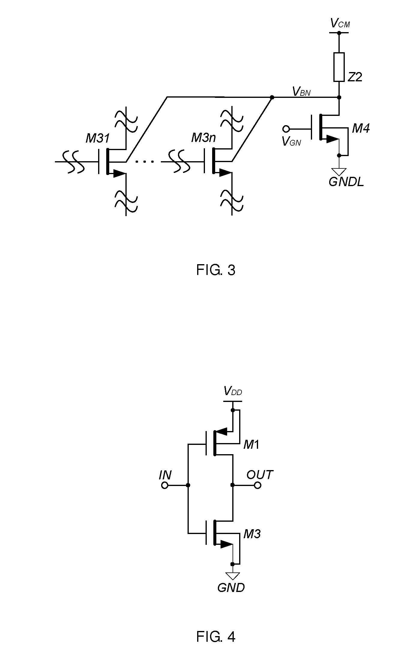
[0042]The key element of the method for reducing the effects of process, supply voltage and temperature variations according to the present invention lies in body modulation. As we known, the threshold voltage (VT) of a MOS transistor satisfies the following relationship:

VT=VT0+γ(√{square root over (2|φF|+vSB)}−√{square root over (2|φF|)})

where vSB is the source-body voltage of the MOS transistor, VT0 is the threshold voltage when vSB=0, γ is body threshold parameter, and φF is referred to...


PUM


Abstract

This invention provides a method for reducing the effects of process, supply voltage and temperature variations in integrated circuits and its circuit implementation. The disclosed method builds up a detecting-feedback loop with a plurality of target MOS transistors in main circuits, an induction MOS transistor and a current-to-voltage conversion circuit, and performs a body modulation to effectively reduce the parameter fluctuations of the target MOS transistors in a sub-threshold region or a saturated region due to process, supply voltage and temperature variations. A body-modulated circuit achieves the disclosed method with only a few circuit elements, which effectively improves the stability, reliability and product yield of integrated circuits, especially sub-threshold integrated circuits, without significantly increasing the circuit complexity and power consumption.

Description

BACKGROUND OF THE INVENTION[0001]1. Field of the Invention[0002]The present invention relates to a method for reducing the effects of process, supply voltage and temperature variations in integrated circuits and its circuit implementation, and in particular, to a method building up a detecting-feedback loop (with a plurality of target MOS (Metal-Oxide-Semiconductor) transistors, an induction MOS transistor and a current-to-voltage conversion circuit) for performing body modulation to reduce the parameter fluctuations of the target MOS transistors in a sub-threshold region or a saturated region due to process, supply voltage and temperature variations, and a body-modulated circuit for realizing the aforementioned method and its application in integrated circuits, especially in sub-threshold integrated circuits (class-C inverter, inverter-based integrator, inverter-based ΣΔ (Sigma-Delta) modulator, etc.).[0003]2. Description of the Related Art[0004]The rapid development of portable el...

Claims


Application Information

Patent Timeline
IPC IPC(8): H01L37/00G05F1/10
CPCG05F3/205H03F1/30H03M3/418H03M3/356H03F3/217
Inventor LUO, HAOHAN, YANHAN, XIAOXIALIU, XIAOPENG
Owner LUO HAO
Why Eureka
Try Eureka