Method for producing core-shell nanowires, nanowires produced by the method and nanowire device comprising the nanowires

a nanowire and nanowire technology, applied in nanoinformatics, instruments, optical elements, etc., can solve the problems of inability to achieve a three-dimensional vertical structure, no satisfactory results are achieved in the development of a technology,

Active Publication Date: 2010-12-30
SAMSUNG ELECTRONICS CO LTD
View PDF20 Cites 86 Cited by
  • Summary
  • Abstract
  • Description
  • Claims
  • Application Information

AI Technical Summary

Benefits of technology

[0011]Example embodiments provide a method for producing core-shell nanowires whose density and position is controllable in a simple manner.

Problems solved by technology

However, no satisfactory results are achieved in developing a technology to arrange nanowires at desired positions of substrates to fabricate devices.
The prior art involves complicated processing steps, i.e. separation and arrangement of the nanowire structures, formation of electrodes on the nanowire structures and etching of the nanowire structures.
Another drawback of the prior art is that the nanowire structures are arranged in a two-dimensional configuration, thus making it impossible to attain a three-dimensional vertical structure, which is an important advantage of nanowires.

Method used


Image

  • Method for producing core-shell nanowires, nanowires produced by the method and nanowire device comprising the nanowires
  • Method for producing core-shell nanowires, nanowires produced by the method and nanowire device comprising the nanowires
  • Method for producing core-shell nanowires, nanowires produced by the method and nanowire device comprising the nanowires

Examples


example 1

Production of Silicon Nanowires

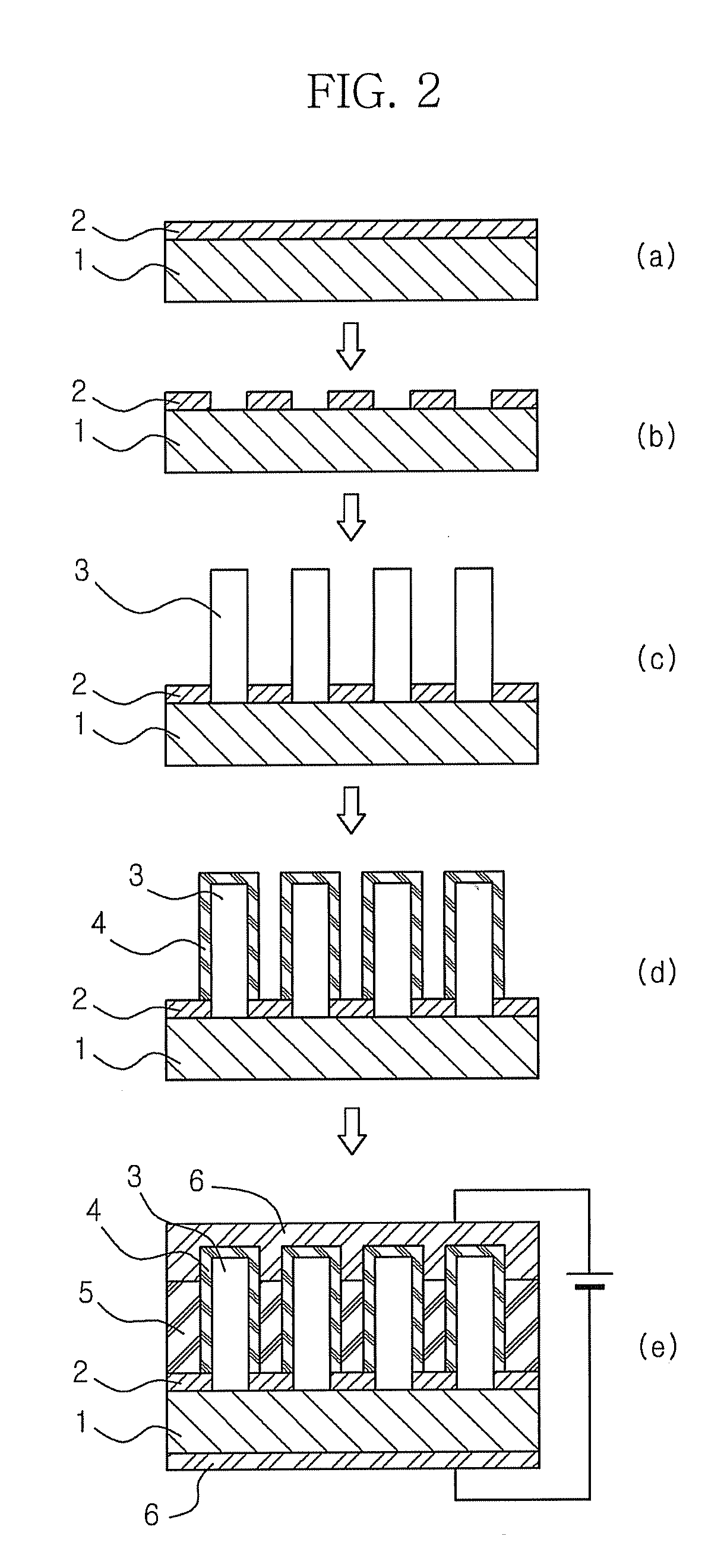
[0101]A natural oxide film of an electrically conductive silicon substrate was removed by cleaning with an organic solvent and hydrofluoric acid. Gold (Au) nanoparticles (Nipponpaint) as catalysts were spin-coated or E-beam deposited on the clean silicon substrate to form a thin film having a thickness of about 30 nm. A SiO2 oxide film was deposited to a thickness of 1 μm on the thin film. Thereafter, a photoresist (AZ-1512, Clariant) was spin-coated on the SiO2 oxide film, exposed to light using a UV-exposure system (Oriel) as a light source through a photomask, and developed to form a pattern. The exposed areas of the SiO2 oxide film, from which the photoresist was removed, were etched with a hydrofluoric acid solution to expose areas of the catalyst layer. Subsequently, the resulting structure was put into a furnace and heating at a rate of 10-15° C. / min. while feeding diluted SiH4 as a precursor for nanowires and BH3 as a dopant at a flow rate of 1...

example 2

Fabrication of Vertical EL Light Emitting Device

[0102]A vertical EL light emitting device was fabricated by filling polyimide as an insulating material between the nanowires produced in Example 1 and forming ITO electrode layers on top of the first nanowire shells.

example 3

Fabrication of Horizontal EL Light Emitting Device

[0103]A horizontal EL light emitting device was fabricated by removing the substrate from the nanowires produced in Example 1 to leave the nanowires only, arranging the nanowires parallel to one another, and adhering electrodes to the nanowires.

[0104]According to the method of exemplary embodiments, core-shell nanowires whose density and position is controllable can be produced in a simple manner. The vertical arrangement of the nanowires in a three dimensional array leads to an increase in light emitting / receiving area, which enables the fabrication of high-luminance and high-efficiency devices. In addition, the intervals of the nanowires can be controlled to achieve photonic crystal effects.


PUM

PropertyMeasurementUnit
thicknessaaaaaaaaaa
lengthaaaaaaaaaa
lengthaaaaaaaaaa

Abstract

Disclosed is a method for producing core-shell nanowires in which an insulating film is previously patterned to block the contacts between nanowire cores and nanowire shells. According to the method, core-shell nanowires whose density and position is controllable can be produced in a simple manner. Further disclosed are nanowires produced by the method and a nanowire device comprising the nanowires. The use of the nanowires leads to an increase in the light emitting/receiving area of the device. Therefore, the device exhibits high luminance/efficiency characteristics.

Description

BACKGROUND OF THE INVENTION[0001]This non-provisional application claims priority under 35 U.S.C. §119 to Korean Patent Application No. 10-2007-0067549, filed on Jul. 5, 2007 in the Korean Intellectual Property Office (KIPO), the entire contents of which are herein incorporated by reference.FIELD OF THE INVENTION[0002]Example embodiments relate to a method for producing core-shell nanowires, core-shell nanowires produced by the method, and a nanowire device comprising the core-shell nanowires. Other example embodiments relate to a method for producing core-shell nanowires whose density and position is controllable by using a previously patterned insulating film to block the contacts between nanowire cores and nanowire shells, nanowires produced by the method, and a nanowire device comprising the nanowires.DESCRIPTION OF THE RELATED ART[0003]Nanowires are linear materials whose diameter is in the nanometer range (1 nm=10−9m) and whose length is much larger than the diameter. Nanowire...

Claims


Application Information

Patent Timeline
Patent Type & Authority Applications(United States)
IPC IPC(8): H01L29/06H01L21/20
CPCB82Y10/00Y10S977/936B82Y30/00B82Y40/00G02B2207/101H01L21/0237H01L21/02521H01L21/02603H01L21/02642H01L33/0012H01L33/08H01L33/24H01L33/507Y10S977/742Y10S977/762Y10S977/891B82Y20/00B82B3/00
Inventor LEE, EUN KYUNGHAN, JAI YONGCHOI, BYOUNG LYONGCHO, KYUNG SANG
Owner SAMSUNG ELECTRONICS CO LTD
Why Eureka
Try Eureka