Semiconductor device on direct silicon bonded substrate with different layer thickness

a technology of silicon bonded substrate and silicon bonded layer, which is applied in the direction of semiconductor devices, electrical devices, transistors, etc., can solve the problems of high junction leakage current, and achieve the effects of improving hole mobility, reducing junction leakage current, and increasing thickness

Inactive Publication Date: 2010-12-30
KK TOSHIBA
View PDF15 Cites 7 Cited by
  • Summary
  • Abstract
  • Description
  • Claims
  • Application Information

AI Technical Summary

Benefits of technology

[0006]One aspect of the subject innovation relates to a Direct Silicon Bonded (DSB) substrate with two or more layers (e.g., substrates), wherein a thickness related to at least one layer is adjusted and formed based upon an amount of threshold voltage (Vt). A high threshold voltage (HVt) can correspond to a greater thickness of a substrate in comparison to a low threshold voltage (LVt). Thus, a HVt substrate can have a greater thickness than a LVt substrate in order to improve hole mobility and mitigate junction leakage.

Problems solved by technology

Yet, the bonded interface between the two layers that are DSB together can cause high junction leakage current.

Method used


Image

  • Semiconductor device on direct silicon bonded substrate with different layer thickness
  • Semiconductor device on direct silicon bonded substrate with different layer thickness
  • Semiconductor device on direct silicon bonded substrate with different layer thickness

Examples


Embodiment Construction

[0016]The following is a description of embodiments of the subject innovation, with reference to the accompanying drawings. The accompanying drawings are schematic views designed to facilitate explanation and understanding of the innovation. The shapes, sizes, and ratios shown in the drawings might be different from those of the actual devices, but they may be arbitrarily changed or modified, with the following description and the conventional techniques being taken into account.

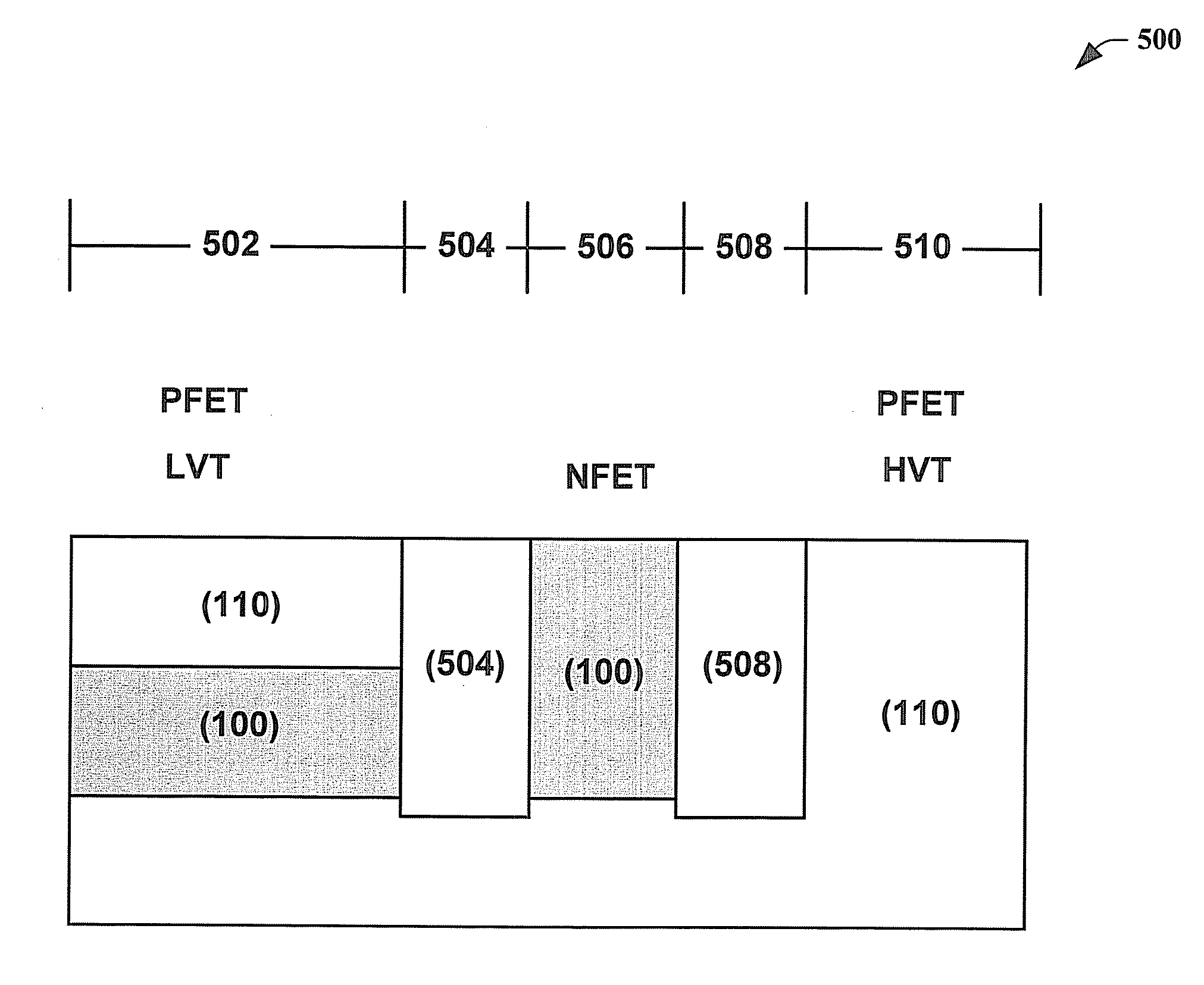
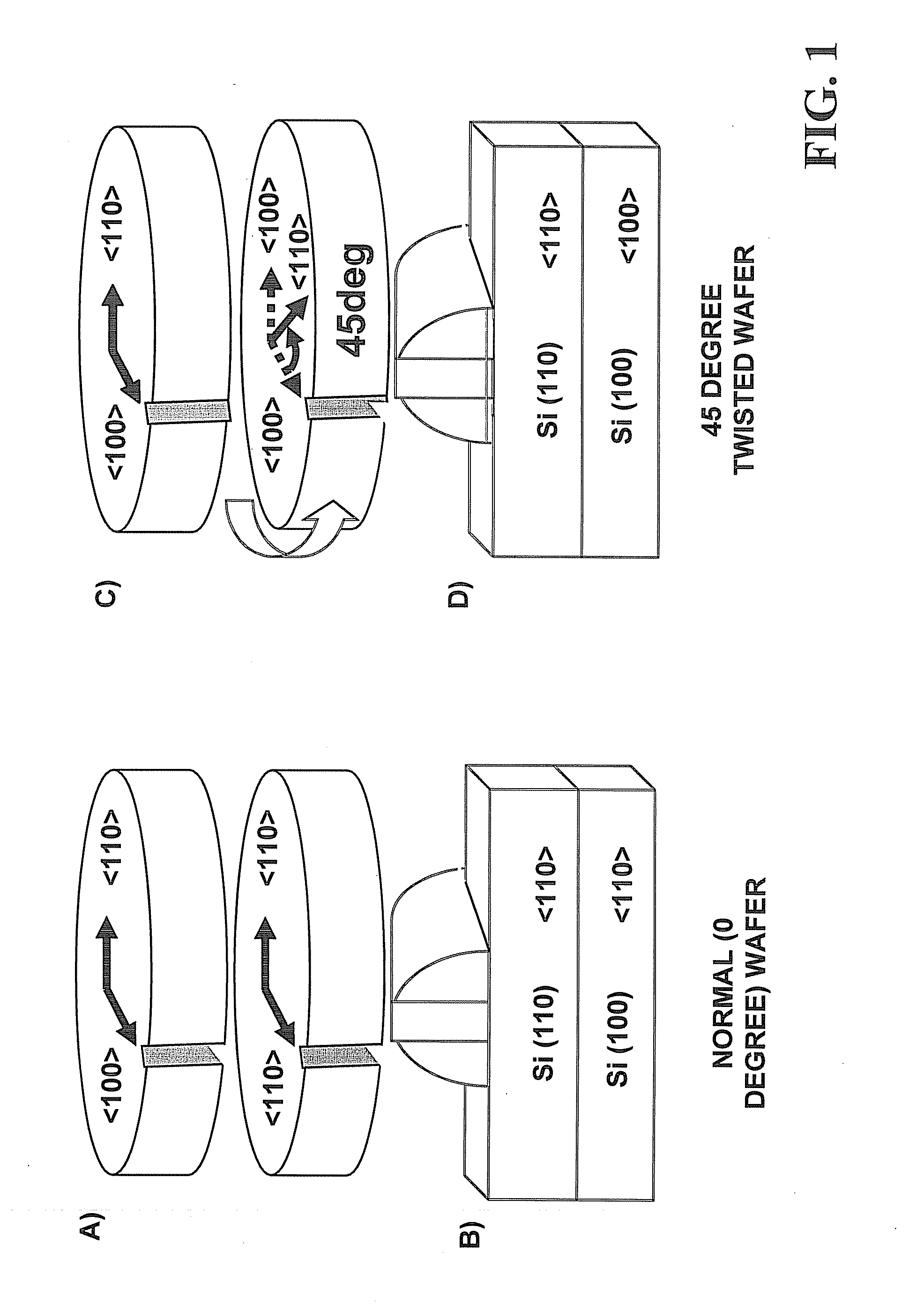
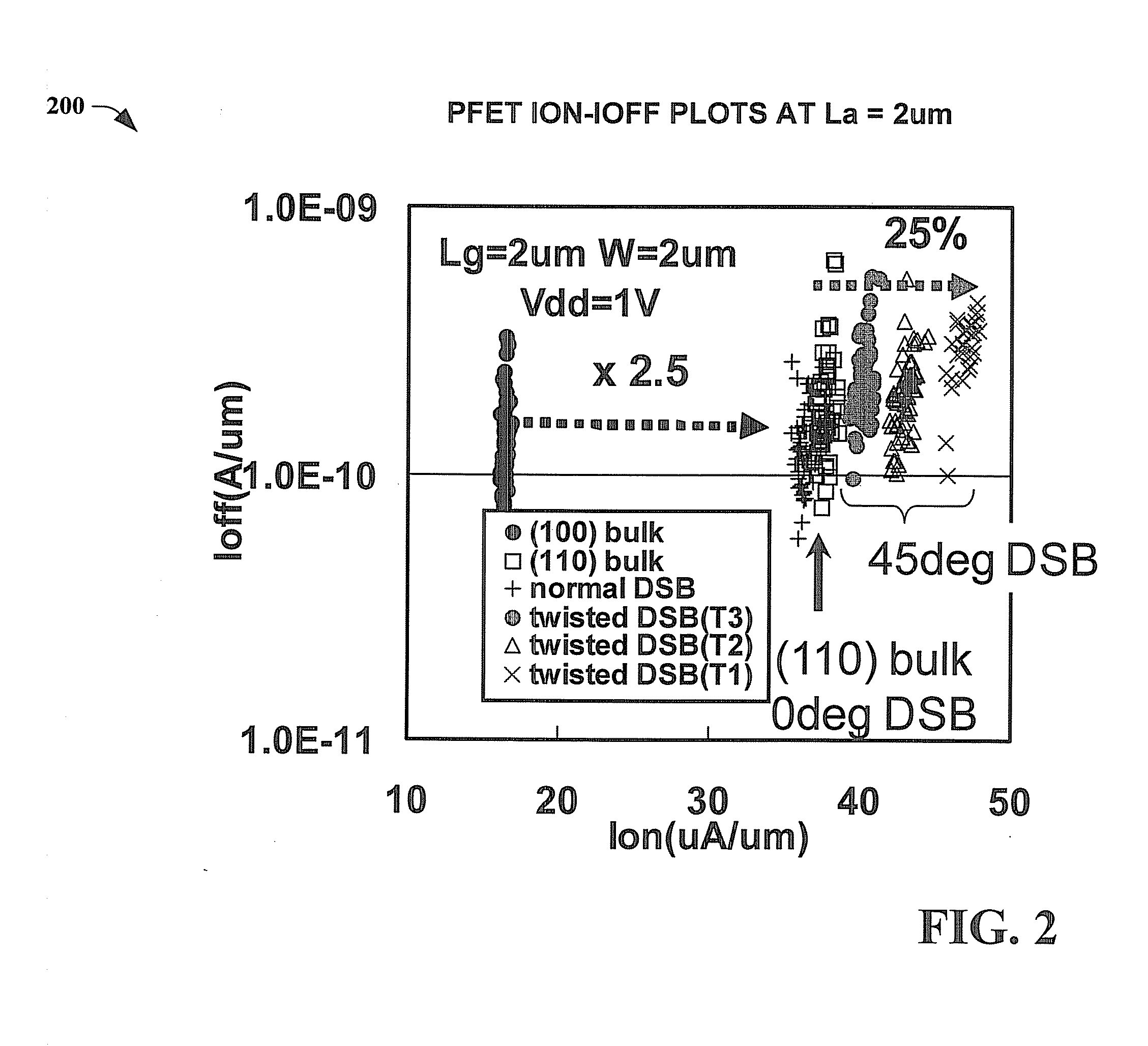
[0017]The subject innovation mitigates high junction leakage while gaining improved hole mobility in a Direct Silicon Bonded (DSB) substrate. Typically, a DSB substrate can include at least two layers that are directly bonded together in which one layer can be twisted to an azimuthal twist angle of 45 degrees. With the twist angle of 45 degrees, higher hole mobility is reflected—yet high junction leakage exists at the bonded interface. The subject innovation mitigates such high junction leakage by varying DS...


PUM


Abstract

A Direct Silicon Bonded substrate can include a first substrate and a second substrate in which the second substrate can be rotated to an azimuthal twist angle of 45 degrees in comparison to the first substrate. Disclosed are a semiconductor device and a method for making a semiconductor device that includes a DSB substrate with an adjusted thickness based upon the threshold voltage (Vt). In other words, a thicker substrate or layer can correspond to a high threshold voltage (HVt) and a thinner substrate or layer can correspond to a low threshold voltage (LVt) in order to improve mobility in LVt devices.

Description

TECHNICAL FIELD[0001]The present invention relates to a semiconductor device on Direct Silicon Bonded (DSB) substrate in which layer thickness is adjusted based on an amount of threshold voltage (Vt).BACKGROUND[0002]A semiconductor device using a direct bond substrate, for example, a substrate having a direct silicon bond (DSB) has a structure in which hybrid-orientation-technology can be used and which does not have a silicon-on-insulator (SOI) structure. The DSB substrate does not have buried oxide (BOX) unlike the SOI substrate. Therefore, ideally, nothing other than silicon is provided on an interface on which silicon layers having different plane orientations (crystal orientations) are bonded together.[0003]Direct Silicon Bonded (DSB) is a bulk CMOS hybrid orientation technology that can exploit the higher electron and hole mobility expected from Silicon surfaces. Regarding hybrid orientation fabrication and technology, a twist-angle-optimized direct silicon bonded substrate ca...

Claims


Application Information

Patent Timeline
Patent Type & Authority Applications(United States)
IPC IPC(8): H01L29/06H01L21/76H01L21/18
CPCH01L21/02381H01L21/02433H01L21/02532H01L21/02609H01L21/02639H01L29/1054H01L21/187H01L21/26506H01L21/823412H01L21/823807H01L29/045H01L21/02667
Inventor HAMAGUCHI, MASAFUMIHASUMI, RYOJI
Owner KK TOSHIBA
Why Eureka
Try Eureka