Output buffer circuit and output buffer system

a buffer circuit and output technology, applied in the direction of circuit arrangements, emergency protective circuit arrangements, transistors, etc., can solve the problem of overcurrent destroying the switching elements

Inactive Publication Date: 2011-01-06
PANASONIC CORP
View PDF1 Cites 30 Cited by
  • Summary
  • Abstract
  • Description
  • Claims
  • Application Information

AI Technical Summary

Benefits of technology

[0016]The present invention was made to solve these problems, and an object of the present invention is to provide an output buffer circuit capable of surely prevent a switching element of an output circuit from being destroyed by a short circuit, and an output buffer system including a plurality of such output buffer circuits.
[0018]In accordance with this configuration, in a case where the short circuit of the output portion is occurring, a short-circuit current flows through the second output circuit, the output portion, and a short-circuit point. Therefore, the short-circuit current does not flow through the high voltage side switching element and low voltage side switching element of the first output circuit. Moreover, the short-circuit current is suppressed by a current ability of the second output circuit. Therefore, the output circuits (the first output circuit and the second output circuit) can be surely prevented from being destroyed by the short circuit.
[0022]The output buffer circuit may be configured such that the high voltage side output circuit and the low voltage side output circuit are activated at the same time, and the short-circuit detecting circuit is activated. In accordance with this configuration, since the high voltage side output circuit and the low voltage side output circuit are activated at the same time, the short circuit can be detected comparatively quickly.
[0023]The output buffer circuit may be configured such that: one of the high voltage side output circuit and the low voltage side output circuit is activated, and the short-circuit detecting circuit is activated; and when the short circuit is not detected, the other one of the high voltage side output circuit and the low voltage side output circuit is activated, and the short-circuit detecting circuit is activated. In accordance with this configuration, the current of the second output circuit is suppressed as compared to a case where the high voltage side output circuit and the low voltage side output circuit are activated at the same time. Therefore, the short circuit can be detected with low power consumption.
[0031]In accordance with this configuration, in a case where the short circuit is occurring at the first output circuit of any of the output buffer circuits, the entire system can be stopped quickly.
[0032]The present invention is configured as explained above and has an effect of being able to provide an output buffer circuit and an output buffer system, each of which is capable of surely preventing a switching element of an output circuit from being destroyed by a short circuit.

Problems solved by technology

However, in accordance with the configuration of the conventional output control circuit, there is concern that the flow of the overcurrent may destroy the switching elements 104 and 105.

Method used


Image

  • Output buffer circuit and output buffer system
  • Output buffer circuit and output buffer system
  • Output buffer circuit and output buffer system

Examples


embodiment 1

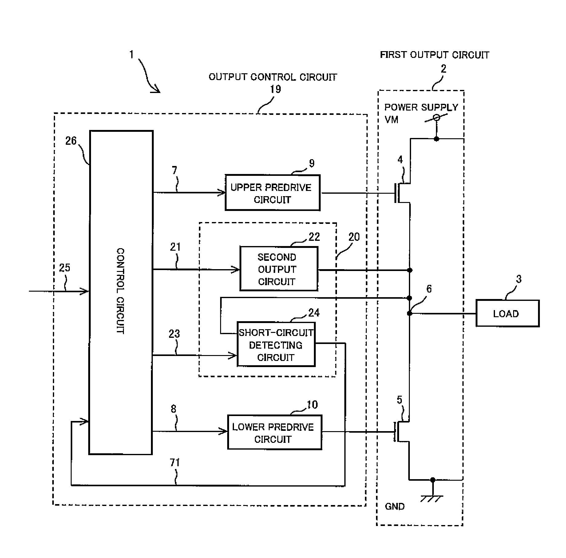
[0049]FIG. 1 is a circuit diagram showing the configuration of an output buffer circuit according to Embodiment 1 of the present invention.

[0050]As shown in FIG. 1, an output buffer circuit 1 includes a first output circuit 2 and an output control circuit 19 configured to control the first output circuit 2.

[0051]The first output circuit 2 includes an upper switching element (first high voltage side switching element) 4 and a lower switching element (first low voltage side switching element) 5, which are connected to each other in series between a power supply VM and a GND. Here, in the present invention, for convenience sake, terminals of each switching element are defined as below. A pair of terminals, through which a current flows in and flows out the switching element, are defined as main terminals, the current being allowed to flow through or being blocked by the switching element by turning on or off the switching element. Moreover, a terminal, to which a control signal for con...

embodiment 2

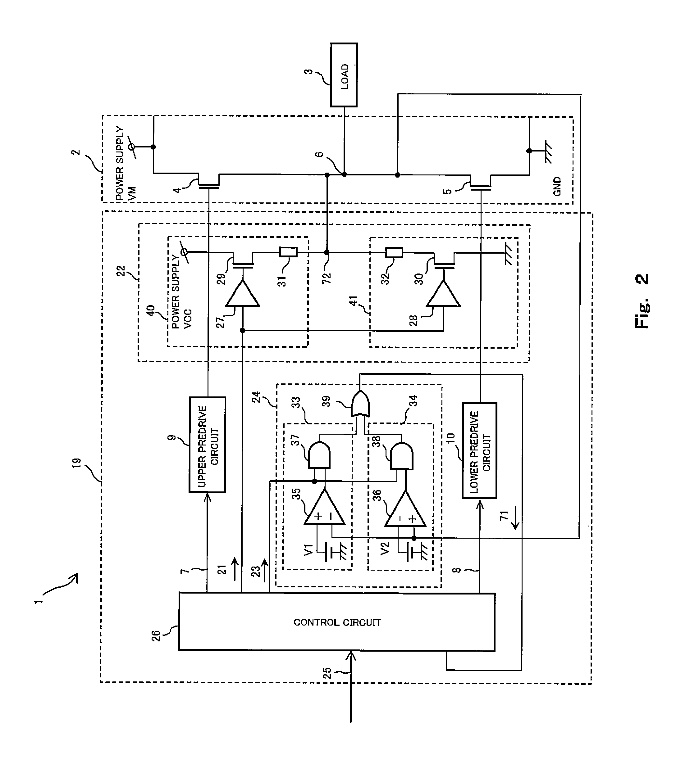
[0094]FIG. 7 is a circuit diagram showing the configuration of the output buffer circuit according to Embodiment 2 of the present invention.

[0095]As shown in FIG. 7, in the output buffer circuit 1 of the present embodiment, the upper output circuit 40 and the lower output circuit 41 are separately controlled by the control circuit 26, and the short-to-ground detecting circuit 33 and the short-to-power detecting circuit 34 are separately controlled by the control circuit 26. Other than these, the output buffer circuit 1 of the present embodiment is the same as the output buffer circuit 1 of Embodiment 1.

[0096]More specifically, an output control circuit 42 of the output buffer circuit 1 of the present embodiment includes a second output circuit 43 instead of the second output circuit 22 of the output control circuit 19 of Embodiment 1. The second output circuit 43 includes the upper output circuit 40 and the lower output circuit 41, which are configured to be the same as those of Emb...

embodiment 3

[0120]Embodiment 3 of the present invention is a variation of Embodiment 2. The configuration of the output buffer circuit 1 of the present embodiment is completely the same as the configuration of the output buffer circuit 1 of FIG. 7. However, when detecting the short circuit, the upper output circuit 40 and the lower output circuit 41 are similarly turned on and off as with Embodiment 1. Moreover, when the short circuit is not detected, the second output circuit 43 is activated at the same timing as the first output circuit 2 in a complementary manner.

[0121]Hereinafter, the operation of the output buffer circuit 1 of the present embodiment will be explained in reference to FIG. 9.

[0122]FIG. 9 is a flow chart showing steps of the operation control by the control circuit 26 of the output buffer circuit 1 of the present embodiment.

[0123]As shown in FIG. 9, Steps S1 to S5 and S7 are the same as those in the flow chart of FIG. 3 of Embodiment 1. Therefore, the output buffer circuit 1 ...


PUM


Abstract

An output buffer circuit of the present invention includes: a first output circuit having a first upper switching element and a first lower switching element, the first upper switching element having main terminals, one of the main terminals being maintained at a first voltage, the first lower switching element having main terminals, one of the main terminals being connected to the other main terminal of the upper switching element, the other main terminal of the first lower switching element being maintained at a second voltage, a portion where the other main terminal of the first upper switching element and one of the main terminals of the first lower switching element are connected to each other constituting an output portion for output to outside; a second output circuit having an output terminal connected to the output portion of the first output circuit; and a short-circuit detecting circuit configured to detect a short circuit of the output portion of the first output circuit. The output buffer circuit of the present invention is configured such that: when starting up the output buffer circuit, the second output circuit and the short-circuit detecting circuit are activated before activating the first output circuit; when the short circuit of the output portion is not detected, the first output circuit is activated; and when the short circuit of the output portion is detected, the first output circuit is not activated.

Description

[0001]This is a continuation application under 35 U.S.C 111(a) of pending prior International application No. PCT / JP2009 / 001726, filed on Apr. 14, 2009. The disclosure of Japanese Patent Application No. 2008-224853 filed on Sep. 2, 2008 including specification, drawings and claims is incorporated here in by reference in its entirety.BACKGROUND OF THE INVENTION[0002]1. Field of the Invention[0003]The present invention relates to an output buffer circuit having a short-circuit detecting function and an output buffer system including a plurality of such output buffer circuits.[0004]2. Description of the Related Art[0005]In the case of realizing the integration of an output circuit configured to drive a load at a comparatively high current such as a power amplifier of an acoustic equipment, an audio output circuit of TV, a motor drive circuit, and the like, such IC is destroyed in some cases by a short circuit between a power supply terminal and an output terminal (such short circuit is...

Claims


Application Information

Patent Timeline
Patent Type & Authority Applications(United States)
IPC IPC(8): H02H3/00
CPCH03F1/523H03K17/0822H03F3/2173
Inventor FUKUDA, DAISUKENAGANO, TETSUYANO, TAKEHIRO
Owner PANASONIC CORP
Why Eureka
Try Eureka