Gate drive voltage boost schemes for memory array

a technology of gate drive voltage and memory array, which is applied in the direction of information storage, static storage, digital storage, etc., can solve the problems of significant reduction of achieve the effect of reducing the life of the cell transistor, high programming current, and high memory cell curren

Active Publication Date: 2011-01-06
TAIWAN SEMICON MFG CO LTD
View PDF6 Cites 6 Cited by
  • Summary
  • Abstract
  • Description
  • Claims
  • Application Information

AI Technical Summary

Benefits of technology

[0008]Magnetic memory elements using the Giant magneto-resistive effect, such as Phase Change RAM and Spin Moment Transfer MRAM, sometimes referred to as Spin Torque Transfer MRAM, require high programming currents. Since these currents are controlled by a cell transistor, a fi

Problems solved by technology

This high gate to source/drain voltage and high memory cell cu

Method used


Image

  • Gate drive voltage boost schemes for memory array
  • Gate drive voltage boost schemes for memory array
  • Gate drive voltage boost schemes for memory array

Examples


Embodiment Construction

[0019]Refer now to the Drawings for a description of the preferred embodiments of this invention. In these descriptions all transistors are field effect transistors and will be described herein simply as transistors.

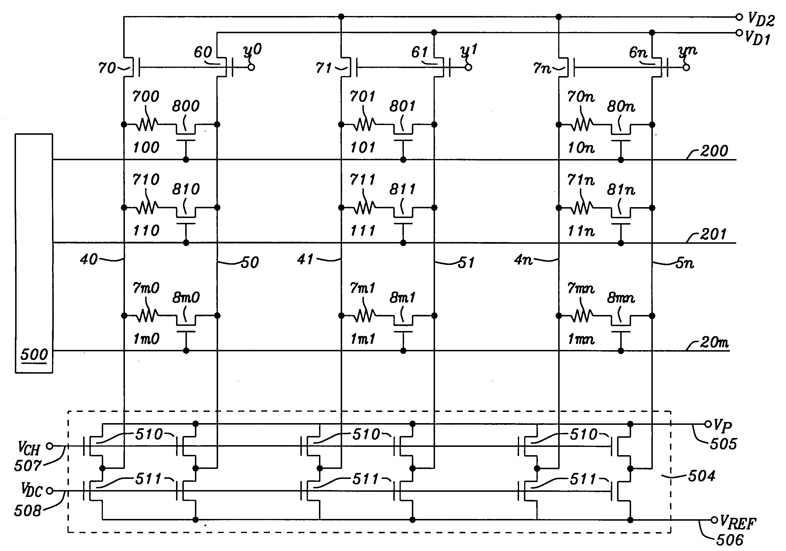
[0020]FIG. 1 shows a schematic drawing of the memory cell array used in this invention. FIG. 1 shows an array of memory cells arranged in rows and columns 100, 101, . . . 10n; 110, 110, . . . , 11n; . . . ; 1m0, 1m1, . . . , 1mn. Each of the memory cells has a magnetic memory element 700, 701, . . . , 70n; 710, 711, . . . , 71n; 7m0, 7m1, . . . , 7mn in series with a cell transistor 800, 801, . . . , 80n; 810, 811, . . . , 81n; 8m0, 8m1, . . . , 8mn. These magnetic memory elements 700, 701, . . . , 70n; 710, 711, . . . , 71n; 7m0, 7m1, . . . , 7mn are two terminal devices and can be represented by a resistor, as shown in FIG. 1. Each column of the array has a BLC line 40, 41, . . . , 4n connected to one terminal of each magnetic memory element 7x0, 7x1, . . . , 7xm in th...


PUM


Abstract

This invention describes a circuit and method to limit the stress caused by gate voltages required to write a one or zero in magnetic memory elements using the Giant magneto-resistive effect, such as Phase Change RAM and Spin Moment Transfer MRAM, sometimes referred to as Spin Torque Transfer MRAM, which require high programming currents. The circuit and method selects one cell at a time for writing a one or a zero, different voltages to write a one or a zero, and a precharge circuit to limit the stress on non selected cells.

Description

BACKGROUND OF THE INVENTION[0001](1) Field of the Invention[0002]This invention relates to gate drive voltage for magnetic memory technologies, such as Phase Change RAM and Spin Moment Transfer MRAM, sometimes referred to as Spin Torque Transfer MRAM, cells which require programming currents higher than the minimum cell transistor can provide without degrading the life of the cell transistor. More particularly the invention relates to circuits and methods for programming these cell transistors by applying high gate voltages only to those cell transistors into which a one or zero is being written.[0003](2) Description of Related Art[0004]U.S. Pat. No. 7,046,547 B2 and U.S. Pat. No. 6,961,265 B2 to Witcraft et al. describe methods and apparatus that allow data to be stored in a magnetic memory cell, such as a giant magneto-resistance cell. The inventions describe advantageously winding a word line around a magnetic memory cell to increase the magnetic field induced by the word line.[0...

Claims


Application Information

Patent Timeline
IPC IPC(8): G11C11/14G11C7/00
CPCG11C11/16G11C13/0004G11C13/0061G11C2213/79G11C2013/0071G11C2013/0073G11C13/0069G11C11/1659G11C11/1675
Inventor YANG, HSU KAI
Owner TAIWAN SEMICON MFG CO LTD
Why Eureka
Try Eureka