Trench MOSFET structures using three masks process

a mosfet and mask technology, applied in the field of cell structure and device configuration of semiconductor devices, can solve the problems of difficult turning and reduced emitter injection efficiency of parasitic npn, and achieve the effect of reducing the area occupied by cells and reducing the size of devices

Active Publication Date: 2011-01-13
FORCE MOS TECH CO LTD
View PDF2 Cites 28 Cited by
  • Summary
  • Abstract
  • Description
  • Claims
  • Application Information

AI Technical Summary

Benefits of technology

[0007]The present invention has been conceived to solve the above-described problems with the related art, and it is an object of the invention to provide

Problems solved by technology

Therefore, a Source Ballast Resistance (SBR) of said n region exists at cell corners, which reduces the Emitter injection efficiency of the pa

Method used


Image

  • Trench MOSFET structures using three masks process
  • Trench MOSFET structures using three masks process
  • Trench MOSFET structures using three masks process

Examples


Embodiment Construction

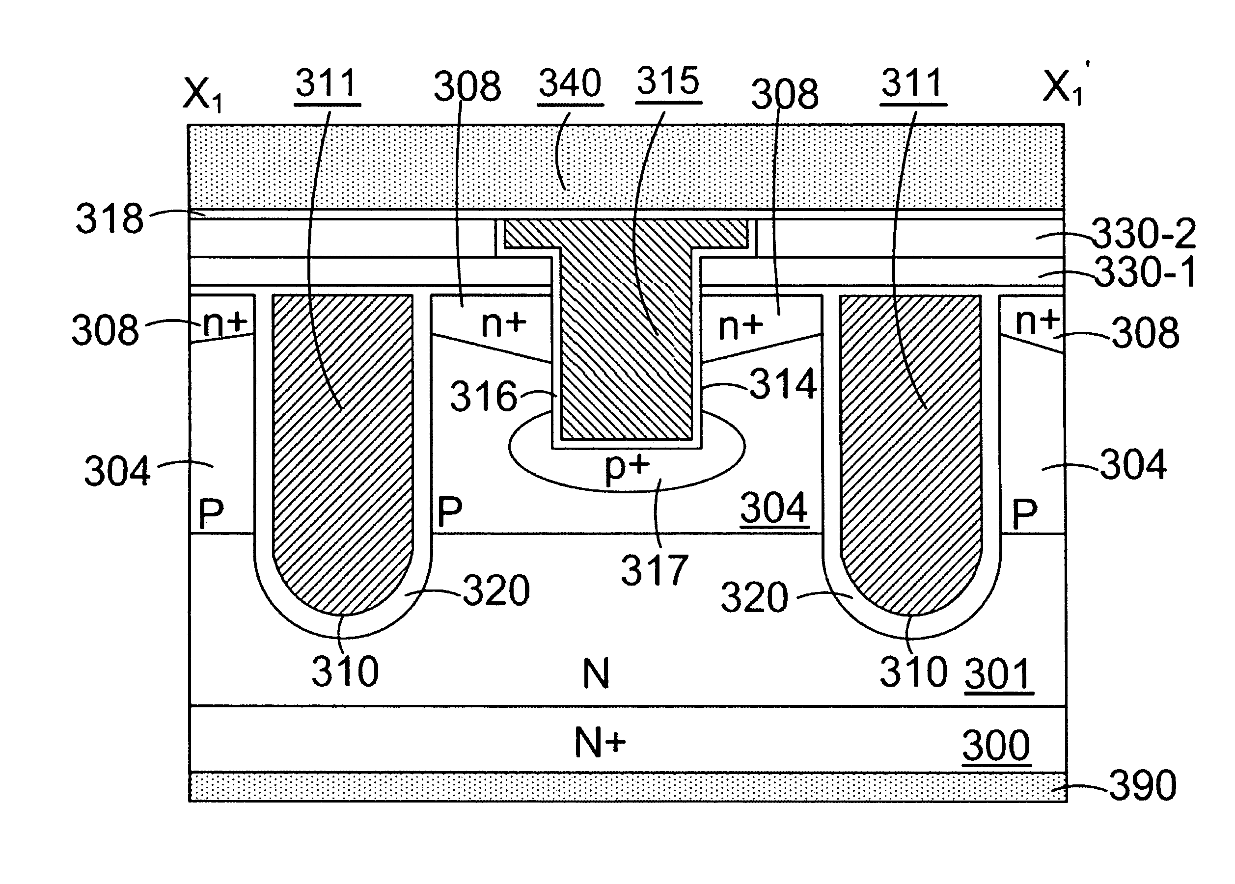
[0049]Please refer to FIG. 3A for a preferred embodiment of this invention, which also is the X1-X1′ cross section of FIG. 2B, where an N-channel trench MOSFET is formed on an N+ substrate 300 coated with back metal 390 of Ti / Ni / Ag on rear side as drain electrode. Onto said N+ substrate 300, a lighter doped N epitaxial layer 301 is grown, and a plurality of first trenched gates 310 filled with doped poly 311 onto a gate oxide 320 are formed wherein. Near the top surface of P body regions 304, n+ source regions 308 are formed with Gaussian-distribution from the open region of trenched source-body contact 314 to channel region near said first trenched gate 310. Each of said trenched source-body contacts 314 filled with W (tungsten) plug 315 padded by a barrier layer 316 of Ti / TiN or Co / TiN or Ta / TiN are penetrating through a contact interlayer comprising a layer of un-doped SRO (Silicon Rich Oxide) 330-1 and a layer of BPSG (Boron Phosphorus Silicon Glass) or PSG (Phosphorus Silicon G...


PUM


Abstract

A trench MOSFET structure having improved avalanche capability is disclosed, wherein the source region is formed by performing source Ion Implantation through contact open region of a contact interlayer, and further diffused to optimize a trade-off between Rds and the avalanche capability. Thus, only three masks are needed in fabrication process, which are trench mask, contact mask and metal mask. Furthermore, said source region has a doping concentration along channel region lower than along contact trench region, and source junction depth along channel region shallower than along contact trench, and source doping profile along surface of epitaxial layer has Guassian-distribution from trenched source-body contact to channel region.

Description

CROSS-REFERENCE TO RELATED APPLICATION[0001]This application is a Continuation-In-Part of U.S. patent application Ser. No. 12 / 458,293 of the same inventor, filed on Jul. 8, 2009 entitled “Trench MOSFET structure having improved avalanche capability using three mask process”, which is incorporated herewith by reference.FIELD OF THE INVENTION[0002]This invention relates generally to the cell structure and device configuration of semiconductor devices. More particularly, this invention relates to an improved trenched MOSFET configuration having improved avalanche capability by three masks process.BACKGROUND OF THE INVENTION[0003]Please refer to FIG. 1A for a conventional N-channel trench MOSFET structure of prior art (U.S. Pat. No. 6,888,196) with n+ source regions having same surface doping concentration and junction depth along trenched source-body contact and channel region. The disclosed N-channel trench MOSFET cell is formed in an N epitaxial layer 102 supported on an N+ substrate...

Claims


Application Information

Patent Timeline
IPC IPC(8): H01L29/78H01L21/336
CPCH01L21/823437H01L29/7813H01L27/088H01L29/0696H01L29/086H01L29/0869H01L29/1095H01L29/407H01L29/41766H01L29/4236H01L29/4238H01L29/456H01L29/66727H01L29/66734H01L29/7803H01L29/7811H01L21/823462
Inventor HSIEH, FU-YUAN
Owner FORCE MOS TECH CO LTD
Why Eureka
Try Eureka