Radio transmission system and electronic device

a transmission system and electronic device technology, applied in the field of radio transmission systems and electronic devices, can solve the problems of increasing power consumption, limited transmission speed and transmission capacity of signal transmission by electric wiring, and limited transmission speed and transmission capacity, and achieves the effect of simple and inexpensive constitution

Active Publication Date: 2011-01-13
SONY CORP
View PDF9 Cites 43 Cited by
  • Summary
  • Abstract
  • Description
  • Claims
  • Application Information

AI Technical Summary

Benefits of technology

[0012]2) In order to deal with the problem of increasing the speed of transmission data, transmission speed per signal line may be decreased by increasing the number of pieces of wiring and thus achieving signal parallelization. However, this measure leads to an increase of input and output terminals, which results in drawbacks such as complication of a printed board and cable wiring, and an increase in semiconductor chip size.
[0023]That is, in providing a signal interface between the first electronic device and the second electronic device, the transmission object signal is transmitted in a contactless manner by the millimeter wave signal (not transmitted by electric wiring). Preferably, at least signal transmission (signal transmission required to be performed at high speed in particular) is performed in a contactless manner by a communication interface using the millimeter wave signal. In short, signal transmission performed by electric contact (electric wiring) via a mounting structure between the first electronic device and the second electronic device is performed by the millimeter wave signal. By performing signal transmission in the millimeter wave band, it is possible to achieve high-speed signal transmission on the order of Gbps, limit a range covered by the millimeter wave signal (reasons for this will be described in embodiments), and obtain effects due to this nature.
[0029]According to one mode of the present invention, when signal transmission is made in a state of a first electronic device being mounted in a second electronic device, a signal interface with a transmission speed and a transmission capacity that are difficult to achieve by electric wiring can be realized. In that case, casing shape and structure are not complicated because many pieces of wiring as in a case of establishing connection by electric wiring are not required. In addition, because the millimeter wave band is used, signal transmission can be made without using electric wiring, and no disturbance is caused to other electric wiring within the devices.
[0030]A signal interface between the first electronic device and the second electronic device can be constructed by the millimeter wave signal unidirectionally or bidirectionally with a simple and inexpensive constitution without depending on a connector having a large number of terminals or signal wiring.

Problems solved by technology

1) The transmission speed and transmission capacity of signal transmission by electric wiring are limited. For example, LVDS (Low Voltage Differential Signaling) is known as a method for achieving high-speed signal transmission by electric wiring, and applying the mechanism of LVDS is considered. However, recent further increases in capacity and speed of transmission data involve problems such as an increase in power consumption, an increase in effect of signal distortion due to reflection and the like, and an increase in spurious radiation. For example, LVDS is reaching a limit in a case of high-speed (real-time) transmission of video signals (including image pickup signals) and signals of computer images and the like within a device.
2) In order to deal with the problem of increasing the speed of transmission data, transmission speed per signal line may be decreased by increasing the number of pieces of wiring and thus achieving signal parallelization. However, this measure leads to an increase of input and output terminals, which results in drawbacks such as complication of a printed board and cable wiring, and an increase in semiconductor chip size.
3) When electric wiring is used, the wiring becomes an antenna, and causes a problem of electromagnetic field interference. In order to take measures against the problem, the configuration of the electronic device and the card type device is complicated. When wiring is routed for high-speed and high-capacity data, electromagnetic field interference becomes a noticeable problem. In addition, when terminals are made bare in the card type device, there is a problem of electrostatic breakdown.

Method used


Image

  • Radio transmission system and electronic device
  • Radio transmission system and electronic device
  • Radio transmission system and electronic device

Examples


first embodiment

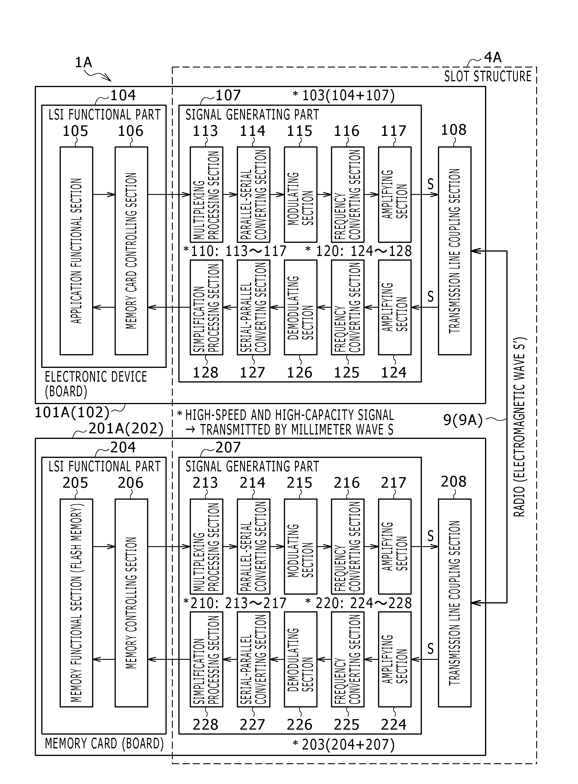
[0130]As shown in FIG. 1, the slot structure 4A according to the first embodiment contributes to the signal generating part 107 and the transmission line coupling section 108 on the electronic device 101A side, the signal generating part 207 and the transmission line coupling section 208 on the memory card 201A side, and the millimeter wave signal transmission line 9 (dielectric transmission line 9A). The dielectric transmission line 9A is provided between the transmission line coupling section 108 and the transmission line coupling section 208.

[0131]Incidentally, unlike a signal interface using related-art electric wiring, the present embodiment flexibly provides for a high-speed characteristic and high capacity by performing signal transmission in the millimeter wave band as described above. For example, in the first embodiment, only signals desired to have a high-speed characteristic and a high-capacity characteristic are set as objects for communication in the millimeter wave ba...

second embodiment

[0168]FIG. 5 is a diagram of assistance in explaining a signal interface in a radio transmission system according to a second embodiment. FIG. 5 is a diagram of assistance in explaining the signal interface in the radio transmission system 1B according to the second embodiment from an aspect of functional configuration.

[0169]The second embodiment makes a millimeter wave signal transmission line 9 a substantial free space. The “substantial free space” means that while the casings of an electronic device 101B and a memory card 201B are a dielectric, a millimeter wave signal is transmitted between the electronic device 101B and the memory card 201B via a transmission line of a free space (free space transmission line 9B) ignoring the dielectric parts.

[0170]In terms of functional configuration, only the dielectric transmission line 9A according to the first embodiment is replaced with the free space transmission line 9B, and the second embodiment is similar to the first embodiment in ot...

third embodiment

[0172]FIG. 6 is a diagram of assistance in explaining a signal interface in a radio transmission system according to a third embodiment. FIG. 6 is a diagram of assistance in explaining the signal interface in the radio transmission system 1C according to the third embodiment from an aspect of functional configuration.

[0173]The third embodiment applies both the dielectric transmission line 9A according to the first embodiment and the free space transmission line 9B according to the second embodiment as the millimeter wave signal transmission line 9. In terms of functional configuration, the third embodiment is a mere combination of the first embodiment and the second embodiment. Therefore description of other parts will be omitted.

[0174]The mechanism of the third embodiment has two systems as millimeter wave signal transmission line 9, and the concept also corresponds to an example of “space division multiplexing” in a fifth embodiment to be described later. While one system of the d...


PUM


Abstract

A radio transmission system includes: a first electronic device; and a second electronic device having a mounting structure mounted with the first electronic device, wherein a millimeter wave signal transmission line capable of transmitting information in a millimeter wave band is formed between the first electronic device and the second electronic device when the first electronic device is mounted in the mounting structure of the second electronic device, and between the first electronic device and the second electronic device, a transmission object signal is converted into a millimeter wave signal and then the millimeter wave signal is transmitted via the millimeter wave signal transmission line.

Description

BACKGROUND OF THE INVENTION[0001]1. Field of the Invention[0002]The present invention relates to a radio transmission system and an electronic device, and particularly to a mechanism of signal transmission between electronic devices when one electronic device is mounted in the other electronic device (on a main unit side, for example).[0003]2. Description of the Related Art[0004]For example, signal transmission may be made in a state of one electronic device being mounted in another electronic device. For example, a card type information processing device typified by a so-called IC card or memory card including a central processing unit (CPU), a nonvolatile storage device (for example a flash memory) and the like can be mounted (detachable) in an electronic device on a main unit side (see Japanese Patent Laid-Open Nos. 2001-195553 and 2007-299338 (hereinafter referred to as Patent Documents 1 and 2)). The card type information processing device as an example of one (first) electroni...

Claims


Application Information

Patent Timeline
Patent Type & Authority Applications(United States)
IPC IPC(8): H04B1/02
CPCG06K19/07749G06K19/07786H01Q1/2275H01Q1/2283H04B1/03H04B5/0025H04B5/0031H04B5/0037H04B7/2606H01Q1/22G06K17/00H04W92/18
Inventor KAWAMURA, HIROFUMI
Owner SONY CORP
Why Eureka
Try Eureka