Method for manufacturing semiconductor substrate, and semiconductor device

a manufacturing method and semiconductor technology, applied in semiconductor devices, electrical equipment, transistors, etc., can solve the problems of silicon carbide itself being the biggest problem, silicon carbide melting, and the inability to manufacture silicon carbide substrates by a high-productivity method, so as to reduce the manufacturing cost of a semiconductor substrate and reduce the manufacturing cost. , the effect of improving the characteristics of a semiconductor elemen

Active Publication Date: 2011-01-20
SEMICON ENERGY LAB CO LTD
View PDF21 Cites 17 Cited by
  • Summary
  • Abstract
  • Description
  • Claims
  • Application Information

AI Technical Summary

Benefits of technology

[0019]According to one embodiment of the disclosed invention, a semiconductor substrate having a silicon carbide layer is manufactured by thinning a silicon carbide substrate. Accordingly, a semiconductor substrate including a silicon carbide layer can be provided at very low cost. In addition, a silicon carbide substrate which is to be a silicon carbide layer can be used a plurality of times; therefore, manufacturing cost for a semiconductor substrate ca...

Problems solved by technology

The cost of a silicon carbide substrate itself is the biggest problem for realizing a semiconductor element using silicon carbide.
It is difficult to melt silicon carbide because of its characteristics; therefore, the silicon carbide substrate cannot be manufactured by a method having high productivity such as a Czochralski (CZ) method or the like which are used for manufacturing a silicon substrate.
Therefore, a sublimation recrystallization method which is disadvantageous in terms of productivity has to be used for manufacturing a silicon carbide substrate for application of semiconductor (for example, see Patent Document 1 and Patent Document 2).
The sublimation recrystallization method is a method in which a material is sublimated by heating and single-crystal silicon carbide is grown on seed crystal; therefore, ...

Method used


Image

  • Method for manufacturing semiconductor substrate, and semiconductor device
  • Method for manufacturing semiconductor substrate, and semiconductor device
  • Method for manufacturing semiconductor substrate, and semiconductor device

Examples


embodiment 1

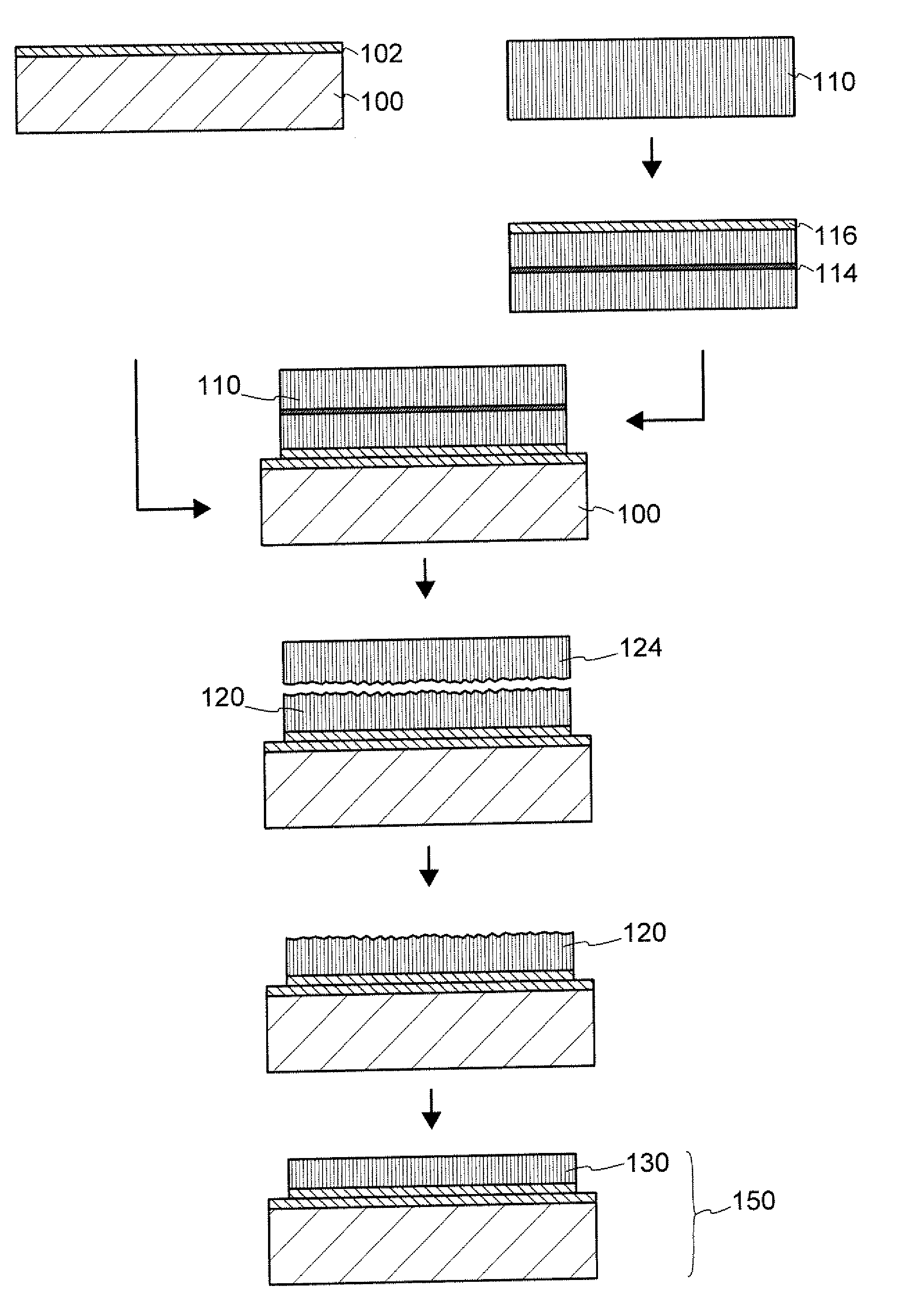
[0034]This embodiment describes an example of a method for manufacturing a semiconductor substrate according to one embodiment of the disclosed invention with reference to FIGS. 1A to 1G.

[0035]First, a base substrate 100 is prepared (see FIG. 1A). Although it is preferable to use a substrate with a high heat resistance, such as a quartz substrate, an alumina substrate, and a silicon substrate as the base substrate 100, a light-transmitting glass substrate used for liquid crystal display devices or the like can be used as long as the light-transmitting glass substrate can withstand heat. In this case, it is preferable to use a substrate having the strain point as high as possible. This embodiment describes the case where the silicon substrate is used as the base substrate 100.

[0036]Note that, as the base substrate 100, as well as the above substrate, a substrate which is formed with an insulator, such as a ceramic substrate or a sapphire substrate; a substrate which is formed with a ...

embodiment 2

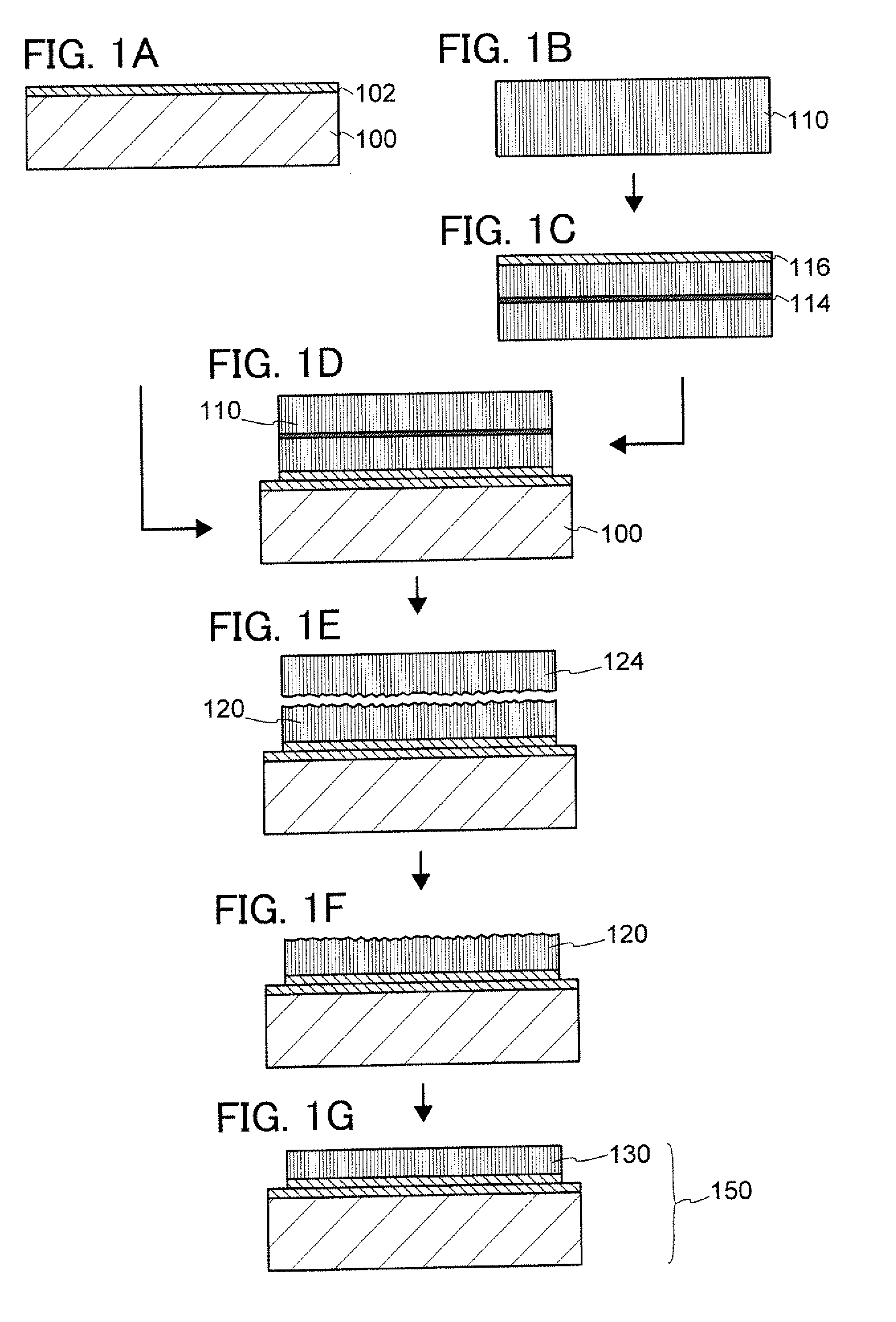
[0067]This embodiment describes another example of a method for manufacturing a semiconductor substrate according to one embodiment of the disclosed invention with reference to FIGS. 2A to 2G. Note that there are many common points between the method for manufacturing a semiconductor substrate in this embodiment and the method for manufacturing a semiconductor substrate, according to the aforementioned embodiment. Therefore, in this embodiment, a method for manufacturing a semiconductor substrate which is different from the method according to the aforementioned embodiment will be described.

[0068]First, a base substrate 100 is prepared and an insulating layer 102 is formed on the surface of the base substrate 100 (see FIG. 2A). Here, the case where a silicon substrate is used as the base substrate 100 and a silicon oxide formed by thermal oxidation treatment is used as the insulating layer 102 is especially described. Needless to say, one embodiment of the disclosed invention is not...

embodiment 3

[0074]This embodiment describes another example of a method for manufacturing a semiconductor substrate according to one embodiment of the disclosed invention with reference to FIGS. 3A to 3G. Note that there are many common points between the method for manufacturing a semiconductor substrate in this embodiment and the method for manufacturing a semiconductor substrate according to the aforementioned embodiment. Therefore, in this embodiment, a method for manufacturing a semiconductor substrate which is different from the methods according to the aforementioned embodiments will be described in detail.

[0075]First, a base substrate 100 is prepared and an insulating layer 102 is formed over the base substrate 100 (see FIG. 3A). The aforementioned embodiment can be referred to for details thereof.

[0076]Next, a silicon carbide substrate 110 is prepared and high conductivity region 112 is formed over the silicon carbide substrate 110 (see FIG. 3B). Note that in this embodiment, the case ...


PUM


Abstract

An object is to provide a novel manufacturing method of a semiconductor substrate containing silicon carbide, and another object is to provide a semiconductor device using silicon carbide. A semiconductor substrate is manufactured through the steps of: adding ions to a silicon carbide substrate to form an embrittlement region in the silicon carbide substrate; bonding the silicon carbide substrate to a base substrate with insulating layers interposed therebetween; heating the silicon carbide substrate and separating the silicon carbide substrate at the embrittlement region to form a silicon carbide layer over the base substrate with the insulating layers interposed between therebetween; and performing heat treatment on the silicon carbide layer at a temperature of 1000° C. to 1300° C. to reduce defects of the silicon carbide layer. A semiconductor device is manufactured using the semiconductor substrate formed as described above.

Description

BACKGROUND OF THE INVENTION[0001]1. Field of the Invention[0002]A technical field of the present invention relates to a method for manufacturing a semiconductor substrate, and a semiconductor device.[0003]2. Description of the Related Art[0004]It is known that silicon carbide as a semiconductor material is more advantageous than silicon in terms of increasing the withstand voltage of a semiconductor element (for example, a transistor), reducing a loss of electric power, or the like. Therefore, it is expected that silicon carbide is used for practical application of a transistor for electric power.[0005]The cost of a silicon carbide substrate itself is the biggest problem for realizing a semiconductor element using silicon carbide. It is difficult to melt silicon carbide because of its characteristics; therefore, the silicon carbide substrate cannot be manufactured by a method having high productivity such as a Czochralski (CZ) method or the like which are used for manufacturing a si...

Claims


Application Information

Patent Timeline
IPC IPC(8): H01L29/78H01L21/762H01L29/24
CPCH01L21/76254H01L21/8213H01L21/84H01L27/12H01L29/0696H01L29/7833H01L29/41766H01L29/66068H01L29/7394H01L29/7812H01L29/7824H01L29/1608
Inventor YAMAZAKI, SHUNPEI
Owner SEMICON ENERGY LAB CO LTD
Why Eureka
Try Eureka