Micromechanically aligned optical assembly

Inactive Publication Date: 2011-01-20
T&S COMM
View PDF10 Cites 63 Cited by
  • Summary
  • Abstract
  • Description
  • Claims
  • Application Information

AI Technical Summary

Benefits of technology

[0030]In one aspect of the invention, the invention provides an optical device, comprising: an input waveguide; an output waveguide; a convex mirror mounted in a holder, the mirror moveable, in the absence of application of means to effectively fix position of the mirror, to reflect light from the input waveguide into the output waveguide; an arm physically coupled to the mirror, the arm having a moveable free end distal from the mirror; and means for effectively permanently fixing position of the mirror.
[0031]In one aspect of the invention, the invention provides an optical device, comprising: a plurality of input waveguides physically coupled to a substrate; a plurality of output wavegui

Problems solved by technology

A challenge of fiber optics has been that packaging and alignment processes are considerably more difficult than electrical wiring.
However, the reach is limited as different modes of the fiber travel at different speeds and it is becomes more difficult to transmit multiple wavelength simultaneously.
Parallel ribbon fibers are of course quite expensive and connectors with 24 fibers inside are complicated to make, even if they use multimode fiber with looser alignment tolerance.
However, none is very effective, especially if multiple sources are coupled into the same fiber.
The disadvantage of this technique is that the fabrication of the laser or semiconductor source becomes more complex, raising the cost.
There is also some sacrifice in the

Method used


Image

  • Micromechanically aligned optical assembly
  • Micromechanically aligned optical assembly
  • Micromechanically aligned optical assembly

Examples


Example

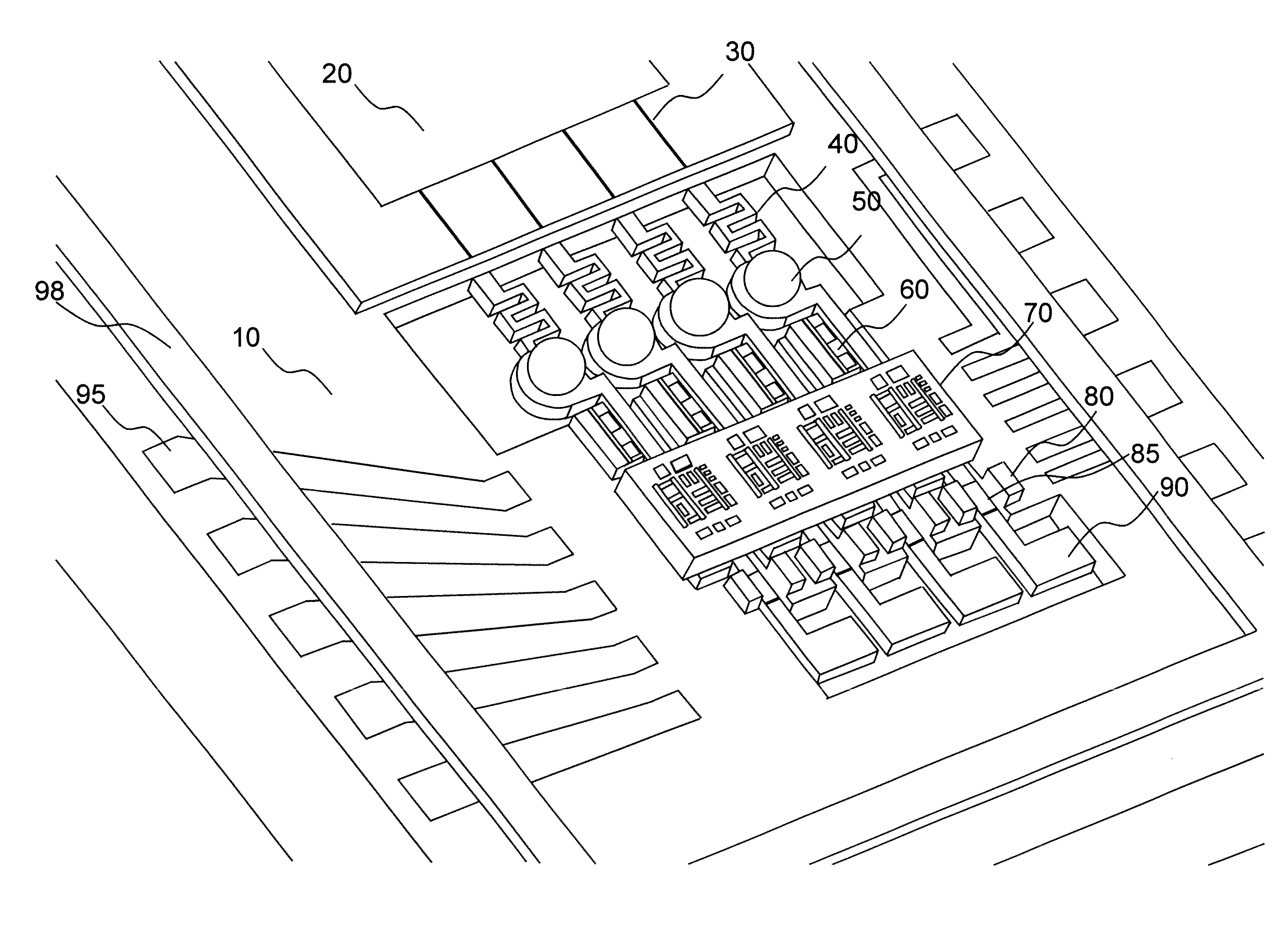
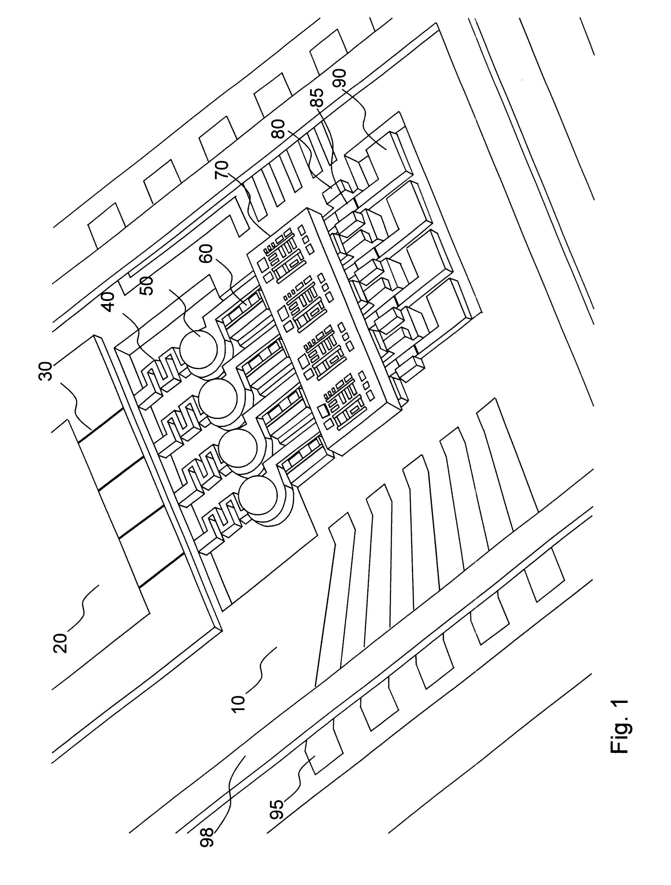
[0057]Aspects of the present invention uses adjustable elements that are integral to the submount to move the optics to optimize the coupling. Once the alignment is perfected or acceptable, the parts are permanently soldered into place using microheaters.

[0058]FIG. 1 shows a laser to PLC coupling part in accordance with aspects of the invention. The entire assembly is mounted on a silicon breadboard or platform 10 that has been suitably prepared for hybrid integration. A PLC multiplexer 20 that combines many wavelengths into one waveguide is mounted on the silicon breadboard. Such a device could be based on etched gratings fabricated in silicon-on-insulator (SOI), or could be based on an Arrayed Waveguide Grating (AWG) fabricated with silica on silicon technology. In either case, there would be a plurality of four as illustrated, input waveguides 30 at one side of the chip and a single waveguide on the other side for output.

[0059]There are also 4 lasers 60 soldered on to the silicon...


PUM

PropertyMeasurementUnit
Lengthaaaaaaaaaa
Poweraaaaaaaaaa
Adhesivityaaaaaaaaaa

Abstract

An optical assembly includes a combination of laser sources emitting radiation, focused by a combination of lenses into optical waveguides. The optical waveguide and the laser source are permanently attached to a common carrier, while at least one of the lenses is attached to a holder that is an integral part of the carrier, but is free to move initially. Micromechanical techniques are used to adjust the position of the lens and holder, and then fix the holder it into place permanently using integrated heaters with solder.

Description

CROSS REFERENCE TO RELATED APPLICATIONS[0001]This application claims the benefit of the filing date of U.S. Provisional Application No. 61 / 148,551, filed Jan. 30, 2009, entitled “Micromechanically Aligned Optical Assembly” the disclosure of which is incorporated by reference.BACKGROUND OF THE INVENTION[0002]The invention relates generally to the fiber optic communications, and more particularly to optical packaging techniques used to align laser sources to optical fibers and other types of waveguides.[0003]Optical fiber communications has generally replaced electrical links over long distances in the past few decades. In more recent past, optical links are being used at shorter distances to connect servers to switches and for datacenters. In the future it is expected as data rates increase and costs of optics decreases that optics will diffuse into computers and the connections within a machine or between processors will be optical. (see for example Kash et al. SPIE Photonics West c...

Claims


Application Information

Patent Timeline
IPC IPC(8): G02B6/32
CPCG02B6/32G02B6/3598G02B6/4214G02B6/4225G02B6/4226Y10T29/49902G02B6/4249F21V14/00F21V14/04Y10T29/49778G02B6/4238G02B6/4207G02B6/4215G02B6/4239G02B6/4244G02B6/4257
Inventor PEZESHKI, BARDIAHEANUE, JOHN
Owner T&S COMM
Why Eureka
Try Eureka