

Method for producing silicon film transferred insulator wafter
Active Publication Date: 2011-01-20
SHIN ETSU CHEM IND CO LTD
View PDF3 Cites 18 Cited by
- Summary
- Abstract
- Description
- Claims
- Application Information
AI Technical Summary
Benefits of technology
[0016]The method for producing a silicon film-transferred insulator wafer of the present invention allows production of the insulator wafer on which a silicon film having favorable uniformity of thickness is transferred without thermal strain, detachment, crack and the like attributed to a difference in thermal expansion coefficients between an insulating substrate and a single crystal silicon wafer.
Problems solved by technology
For this reason, shear stress is generated between the materials which are incompletely bonded to each other so that slippage and crystal defects are induced.
Method used
View moreImage
Smart ImageViewing Examples

Examples
examples
[0056]Hereinbelow, the present invention will be described on the basis of Experiments and Comparative Experiment. However, it should not be construed that the present invention is limited to them below.
Login to View More PUM
 Abstract
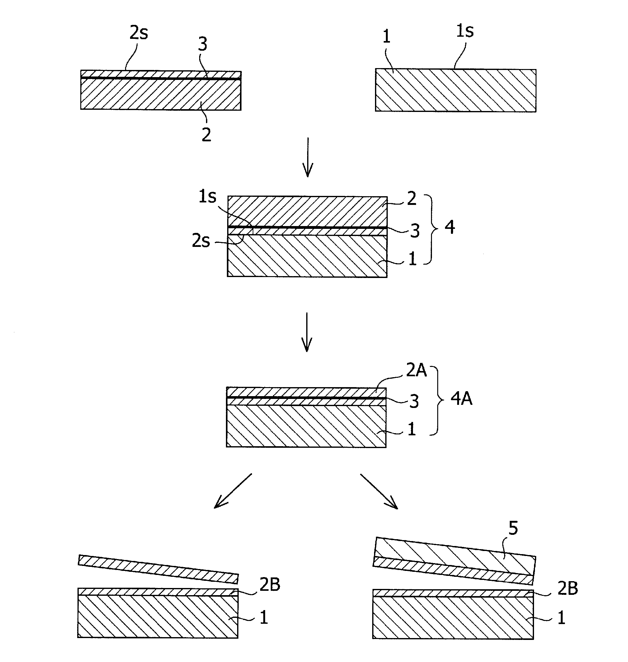
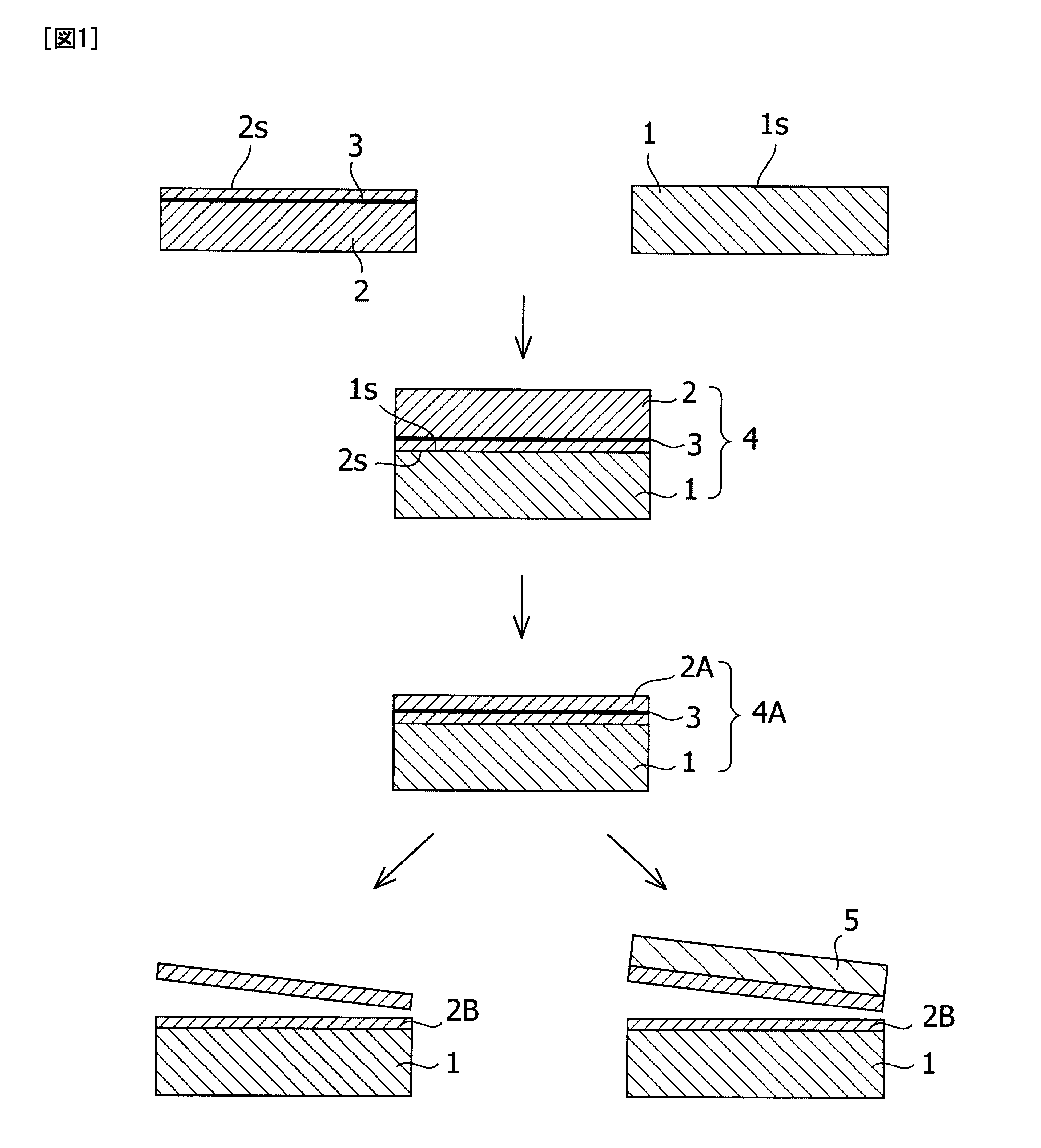
[PROBLEM] Provided is a method for producing an SOI wafer which the method can prevent occurrence of thermal strain, detachment, crack and the like attributed to a difference in thermal expansion coefficients between the insulating substrate and the SOI layer and also improve the uniformity of film thickness of the SOI layer.[MEANS FOR SOLVING THE PROBLEM] Provided is a method for producing an SOI wafer comprising steps of: performing a surface activation treatment on at least one of a surface of an insulator wafer and a hydrogen ion-implanted surface of a single crystal silicon wafer having a hydrogen ion-implanted layer; bonding the hydrogen ion-implanted surface to the surface of the insulator wafer to obtain bonded wafers; heating the bonded wafers at a first temperature; grinding and / or etching a surface of a single crystal silicon wafer side of the bonded wafers thus heated so as to thin the single crystal silicon wafer of the bonded wafers; heating the bonded wafers thus ground and / or etched at a second temperature which is higher the first temperature; and performing detachment at the hydrogen ion-implanted layer by applying a mechanical impact to the hydrogen ion-implanted layer of the bonded wafers thus heated at the second temperature.
Description
TECHNICAL FIELD[0001]The present invention relates to a method for producing a silicon-on-insulator (SOI) wafer.BACKGROUND ART[0002]Conventionally, silicon-on-quartz (SOQ), silicon-on-glass (SOG) and silicon-on-sapphire (SOS) wafers that are collectively referred to as SOI wafers have been devised. Applications of these wafers to projectors, high-frequency devices and so forth have been expected because of the insulation and transparency of handle wafers (quartz, glass, sapphire). Such an SOI wafer is produced by bonding a handle wafer to a silicon wafer (donor wafer).[0003]The conventional SOI fabrication technique includes two main types of bonding processes.[0004]One is called the SOITEC process. In this process, a silicon wafer (donor wafer) into which hydrogen ions have been implanted at room temperature in advance is bonded to a wafer (handle wafer) which serves as a support wafer. Then, the wafers thus bonded are heated at a high temperature (around 500° C.) to generate a lar...
Claims
Login to View More Application Information
Patent Timeline
 IPC IPC(8): H01L21/304
CPCH01L21/76256H01L21/76254
InventorAKIYAMA, SHOJIKUBOTA, YOSHIHIROITO, ATSUOKAWAI, MAKOTOTANAKA, KOUICHITOBISAKA, YUJINOJIMA, YOSHIHIRO
OwnerSHIN ETSU CHEM IND CO LTD