
Infrared light emitting device

a light-emitting device and infrared light technology, which is applied in the manufacture of semiconductor/solid-state devices, semiconductor devices, electrical equipment, etc., can solve the problems of reducing the sensitivity of gas sensors, reducing the intensity of infrared light, and high filter price, so as to reduce the diffusion current of pn diodes and high diode resistance. , the effect of reducing the dark current of the pn diodes

Active Publication Date: 2011-01-27
ASAHI KASEI ELECTRONICS CO LTD
View PDF6 Cites 4 Cited by
  • Summary
  • Abstract
  • Description
  • Claims
  • Application Information

AI Technical Summary

Benefits of technology

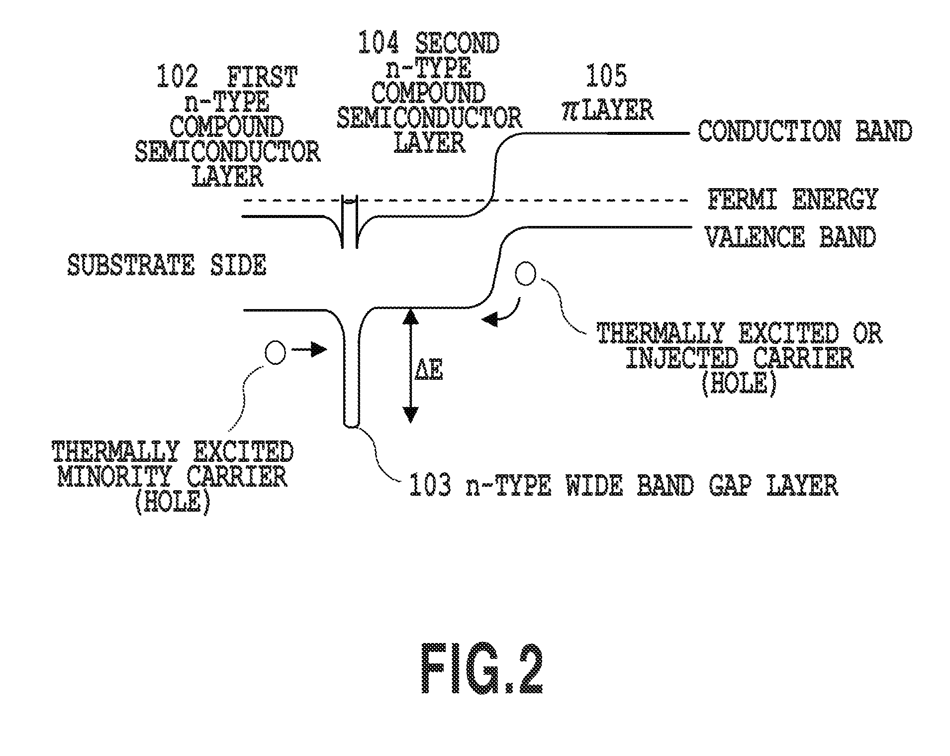
[0026]The present invention can provide an infrared light emitting device with high diode resistance, the device including an n-type compound semiconductor layer and a p-type doped π layer. In the device, an n-type wide band gap layer having a larger band gap than the n-type compound semiconductor layer and the π layer is provided between the n-type compound semiconductor layer and the π layer. This n-type wide band gap layer prevents holes generated in the n-type compound semiconductor layer by thermal excitation at room temperature from diffusing toward the π layer to reduce a dark current in the pn diode due to the holes and to prevent holes generated on the π layer side by thermal excitation from diffusing toward the n-type compound semiconductor layer, thereby reducing a diffusion current in the pn diode.

Problems solved by technology

Such a filter is expensive.
In addition, the filter lowers the intensity of the infrared light, and consequently lowers the sensitivity of the gas sensor.
Moreover, since the incandescent bulb has a short life, the light source needs to be replaced frequently.
However, the device with such a wavelength range is greatly affected by an ambient temperature, and has a trouble in use at room temperature.
Such a semiconductor having a small band gap cannot obtain sufficient pn diode characteristics because thermally excited carriers increase an intrinsic carrier density at room temperature and thereby reduce a device resistance.
However, there is a problem that such a cooling mechanism increases the size and price of the device.

Method used


Image

  • Infrared light emitting device
  • Infrared light emitting device
  • Infrared light emitting device

Examples


embodiment 1

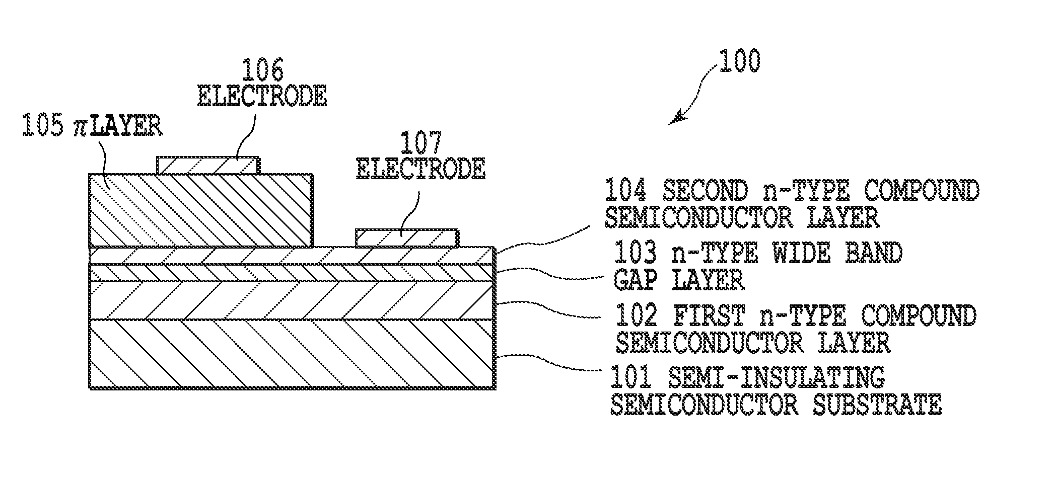
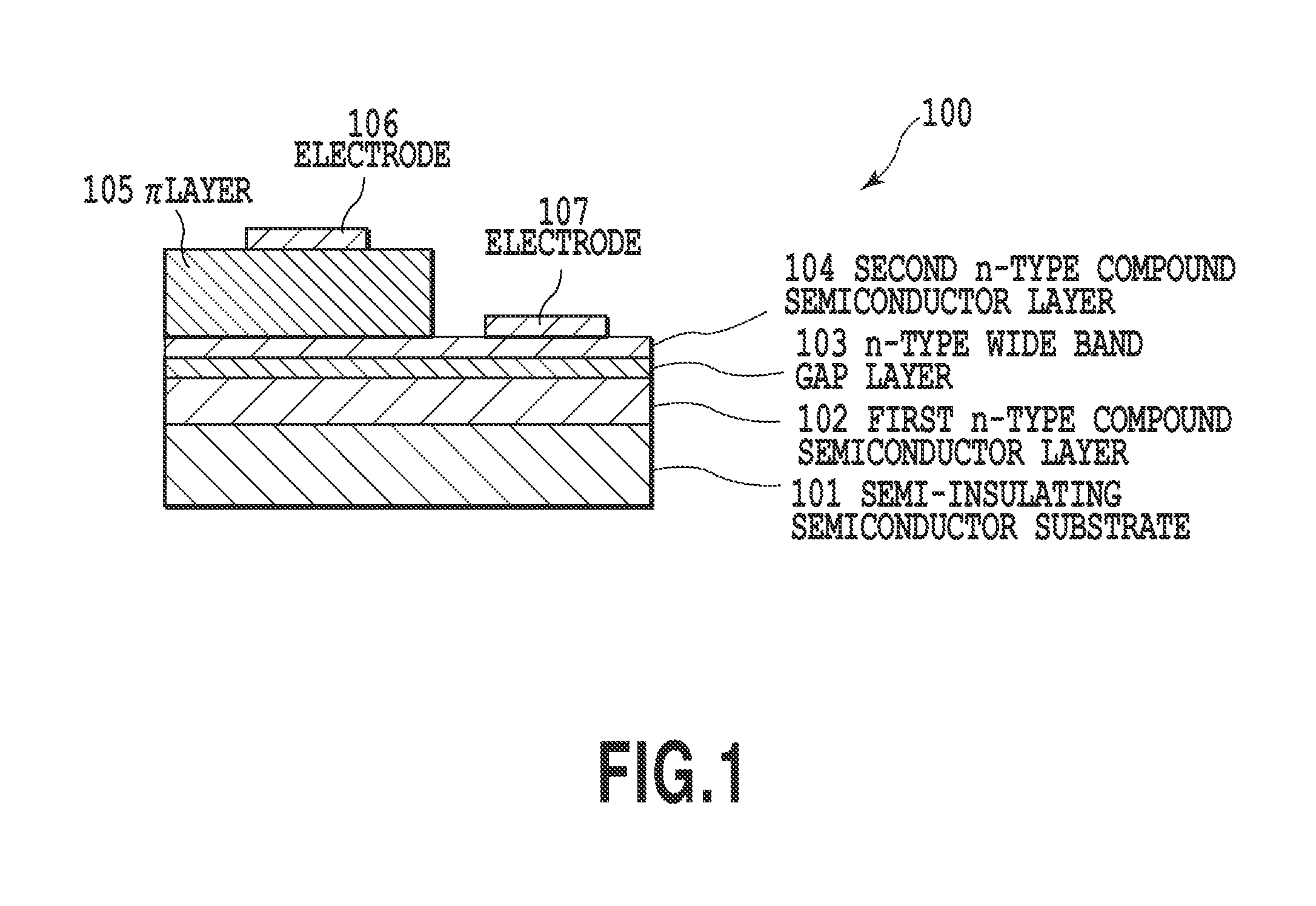
[0046]FIG. 1 is a schematic diagram of an infrared light emitting device according to embodiment 1. An infrared light emitting device 100 includes a semi-insulating semiconductor substrate 101; a first n-type compound semiconductor layer 102 on the semiconductor substrate 101; an n-type wide band gap layer 103 on the first n-type compound semiconductor layer 102; a second n-type compound semiconductor layer 104 on the n-type wide band gap layer 103, the second n-type compound semiconductor layer 104 having the same composition as the first n-type compound semiconductor layer 102; a p-type doped π layer 105 on the second n-type compound semiconductor layer 104; an electrode 106 on the π layer 105; and an electrode 107 on the second n-type compound semiconductor layer 104.

[0047]The infrared light emitting device 100 is a so-called PN junction diode, where a depletion layer is formed between the second n-type compound semiconductor layer 104 and the π layer 105. The infrared light emit...

embodiment 2

[0074]FIG. 6 shows an infrared light emitting device 600 according to embodiment 2. The structure from the semiconductor substrate 101 to the π layer 105 is the same as that of embodiment 1, and similar modifications are conceivable. The infrared light emitting device 600 further includes a p-type compound semiconductor layer 601 which is disposed on the n layer 105, is more heavily p-type doped than the π layer 105, and has the same composition as the first n-type compound semiconductor layer or the π layer. This structure is a so-called PIN diode structure.

[0075]Since the p-type compound semiconductor layer 601 is more heavily p-type doped than the π layer 105, electrons injected from n-type doped layers (101 to 104) side can be more efficiently trapped in the π layer than the example of embodiment 1. As a result, recombination emission efficiency of carriers can be enhanced. Furthermore, the heavy p-type doping can lower contact resistance with an electrode 106. The p-type doping...

embodiment 3

[0076]FIG. 7 shows an infrared light emitting device 700 according to embodiment 3. The structure from the semiconductor substrate 101 to the π layer 105 is the same as that of embodiment 1, and similar modifications are conceivable. The infrared light emitting device 700 further includes a p-type wide band gap layer 701 which is disposed directly on the π layer 105, is more heavily p-type doped than the π layer 105, and has a larger band gap than a first n-type compound semiconductor layer 102 and the π layer 105. This structure is also the so-called PIN diode structure.

[0077]FIG. 8 is a schematic diagram of the energy band gap in the infrared light emitting device according to embodiment 3. By making the band gap of the p-type wide band gap layer 701 to be larger than those of the first n-type compound semiconductor layer 102 and the π layer 105, generation of electrons as minority carriers by thermal excitation in the p-type wide band gap layer 701 can be effectively suppressed. ...


PUM


Abstract

Provided is an infrared light emitting device in which dark current and diffusion current caused by thermally excited holes are suppressed. Thermally excited carriers (holes) generated in a first n-type compound semiconductor layer (102) tend to diffuse in the direction of a π layer (105). But, the dark current by holes is reduced by providing an n-type wide band gap layer (103) with a larger band gap than the first layer (102) and the π layer (105) that suppresses the hole diffusion between the first layer (102) and the π layer (105). The wide band gap layer (103) has a band gap shifted relatively to valence band direction by n-type doping and thereby more effectively functions as a diffusion barrier for the thermally excited holes. Namely, the band gap and n-type doping of the wide band gap layer (103) are adjusted to suppress diffusion of the thermally excited carriers.

Description

TECHNICAL FIELD[0001]The present invention relates to an infrared light emitting device.BACKGROUND ART[0002]Generally, infrared light in a long wavelength range of 3 μm or more is used for human sensors for detecting the presence of a human body, noncontact temperature sensors, gas sensors and the like because of its thermal effect or infrared light absorption effect by gas. Among these application examples, particularly gas sensors have received attention in recent years because they are usable for monitoring and protecting air quality and also for early detection of fire and the like. The principles of the gas sensors using the infrared light are as follows. First, a gas to be measured is injected into a space between an infrared light source and a light receiving device. Since a particular gas absorbs infrared light having a specific wavelength, the type and concentration of the gas can be measured by analyzing wavelength spectrums before and after the injection of the gas. Here,...

Claims


Application Information

Patent Timeline
Patent Type & Authority Applications(United States)
IPC IPC(8): H01L33/08H01L33/02H01L33/32
CPCH01L21/02395H01L21/0254H01L21/02546H01L21/02549H01L21/02573H01L21/02581H01L2924/0002H01L25/0753H01L33/04H01L33/30H01L2924/00
Inventor UENO, KOICHIROKUZE, NAOHIRO
Owner ASAHI KASEI ELECTRONICS CO LTD
Learn More