Semiconductor package and method of manufacturing the same

a semiconductor and package technology, applied in the direction of semiconductor devices, semiconductor/solid-state device details, electrical apparatus, etc., can solve the problems of increasing increasing the demand for miniaturizing circuits, and increasing the complexity of the circuit. , to achieve the effect of improving the signal transmission speed of the semiconductor package, reducing the thickness of the package substrate, and improving the problem of the package substrate bending

Inactive Publication Date: 2011-01-27
SAMSUNG ELECTRO MECHANICS CO LTD
View PDF10 Cites 50 Cited by
  • Summary
  • Abstract
  • Description
  • Claims
  • Application Information

AI Technical Summary

Benefits of technology

[0038]The semiconductor package of the present invention is formed as the coreless package substrate without the core, making it possible to reduce the thickness of the package substrate and improve the signal transmission speed of the semiconductor package.
[0039]In addition, the semiconductor package of the present invention can improve the problem of the bending of the package substrate occurring during the manufacturing process and the productivity of the semiconductor package.
[0040]Moreover, the semiconductor package of the present invention has the passive element and the active element therein, making it possible to improve the rigidity of the semiconductor package.
[0041]Also, the protective member is provided on the lower part of the semiconductor package to protect the passive element that can be exposed to the outside, making it possible to secure the reliability of the semiconductor package.
[0042]Further, the adhesive layer, which is a part of the carrier substrate for manufacturing the semiconductor package, can be used as the protective member or the heat dissipation member of the semiconductor package, making it possible to simplify the process and reduce the process cost.

Problems solved by technology

Therefore, the circuit complexity and density of the package substrate have increased as well as a demand for a miniaturizing circuit has increased.
However, since the circuit layers of a multi-layer on the package substrate are formed on both surfaces of the thick core layer, respectively, by a buildup scheme, there are problems in that the thickness of the package substrate can be thicker and thus, a signal transmission speed between the semiconductor chip and the external circuit unit is degraded.
Since the problem of the bending of the package substrate can cause a bonding default between the semiconductor chip and the package substrate or a bonding fault between the package substrate and the main board substrate, it becomes a factor of degrading the reliability and productivity of the semiconductor package.

Method used


Image

  • Semiconductor package and method of manufacturing the same
  • Semiconductor package and method of manufacturing the same
  • Semiconductor package and method of manufacturing the same

Examples


first embodiment

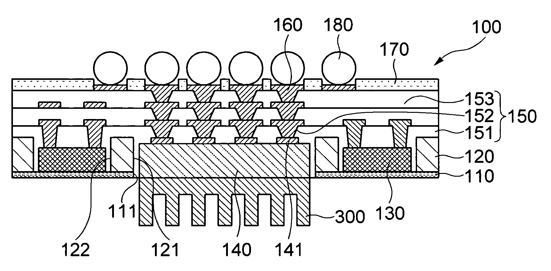
[0052]FIG. 1 is a cross-sectional view of a semiconductor package according to the present invention.

[0053]Referring to FIG. 1, a semiconductor package 100 according to a first embodiment of the present invention may include a protective member 110, insulators 120, an active element 140, passive elements 130, a buildup layer 150, and an external connection unit 180.

[0054]The protective member 110 may be made of an insulating material. For example, the protective member 110 may be made of a solder resist.

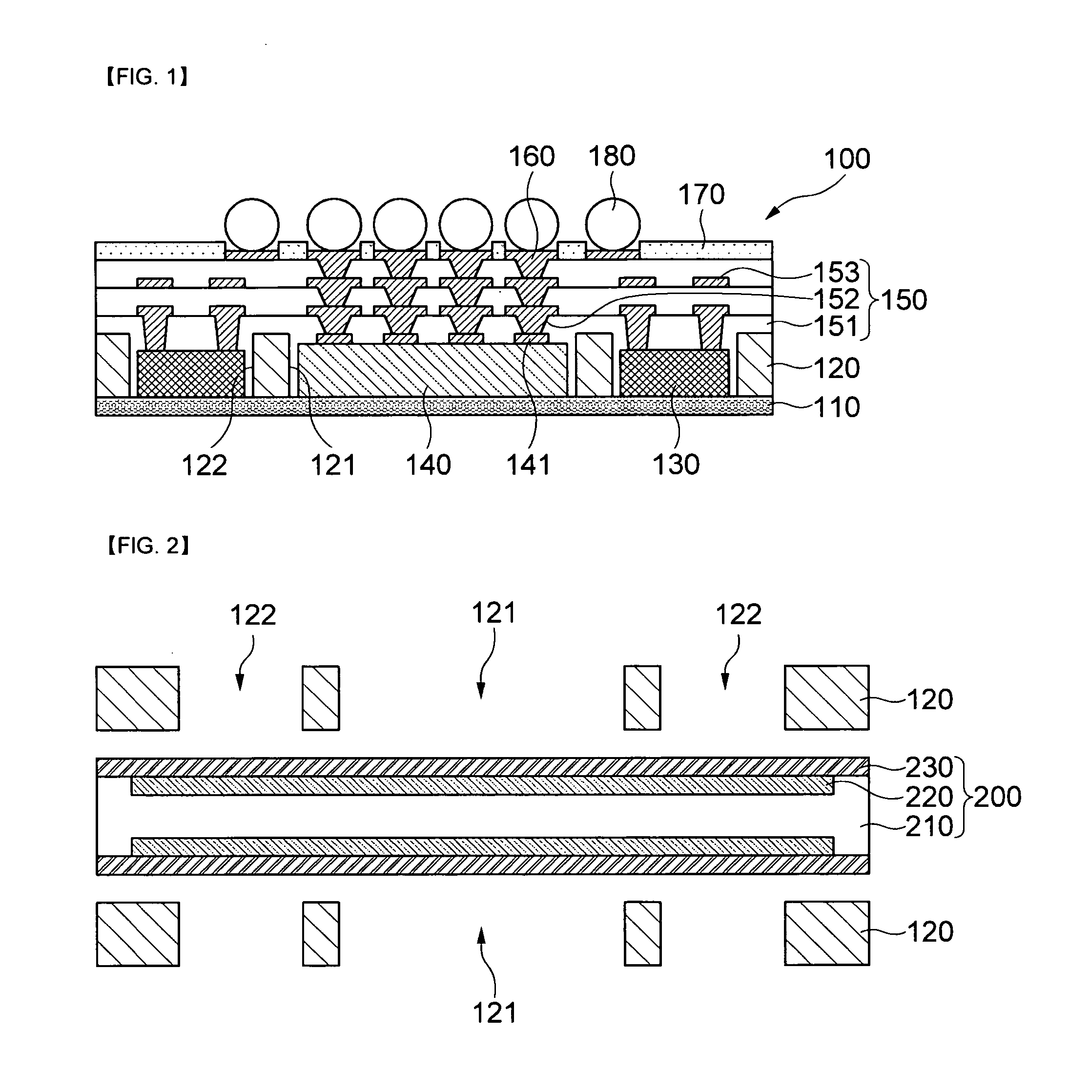
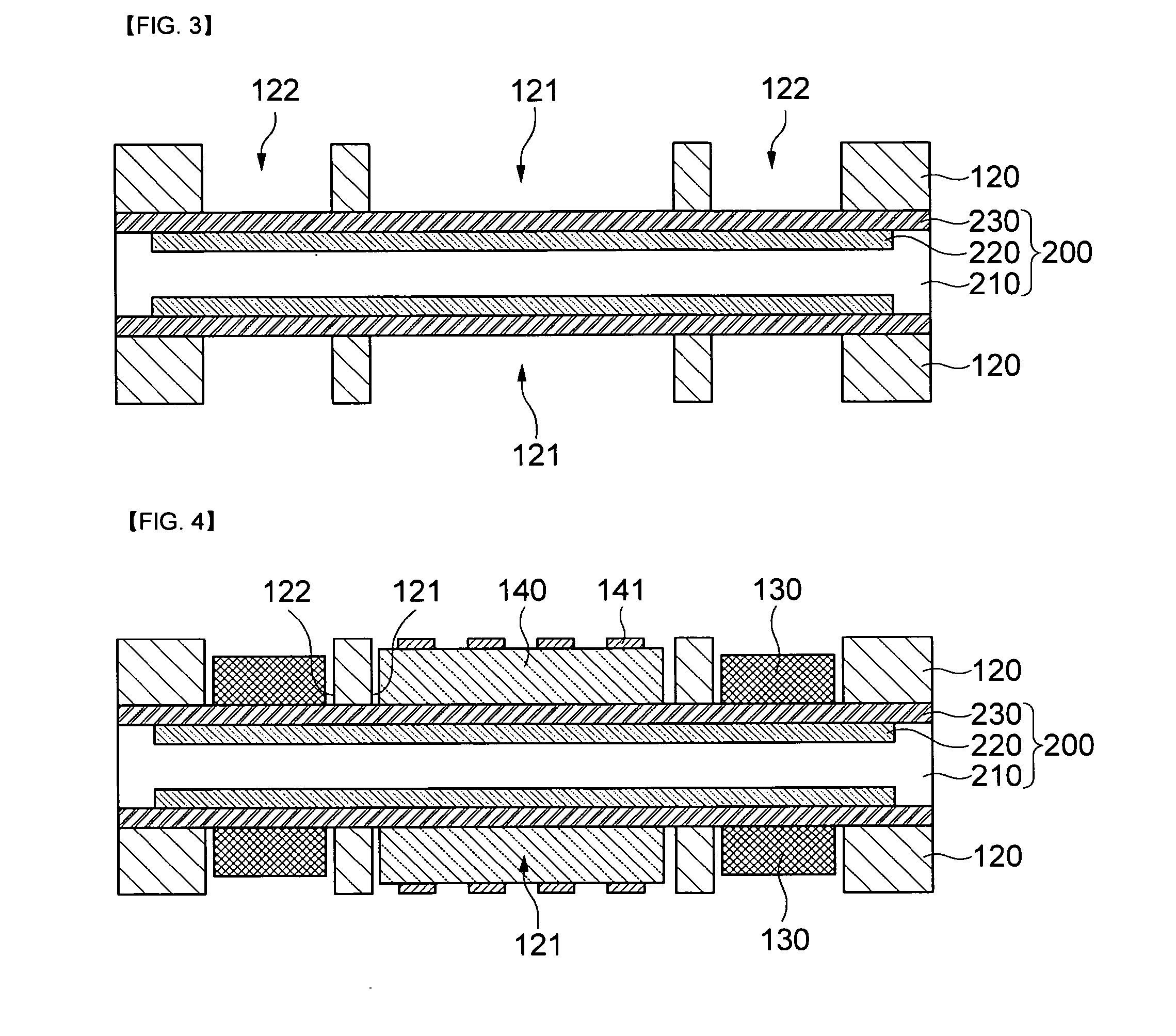
[0055]The insulator 120 is disposed on the protective member 110. The insulator 120 may be made of insulating materials, for example, PPG (Prepreg) or ABF(Ajimonoto buildup film). The insulator 120 may include first and second opening parts 121 and 122 that are penetrated. Herein, the protective member 110 may be exposed from the insulator 120 through the first opening part 121 and the second opening part 122.

[0056]The active element 140 may be disposed on the protective member 110 e...

second embodiment

[0102]FIG. 10 is a cross-sectional view of a semiconductor package according to the present invention.

[0103]Referring to FIG. 10, a semiconductor package according to a second embodiment of the present invention may include the insulator 120 that has the first and second opening parts 121 and 122, the active element 140 that is disposed inside the first opening part 121, the passive element 130 that is disposed inside the second opening part 122, the protective member 110 that covers the lower part of the passive element 130 and is disposed on the lower part of the insulator 120, the buildup layer 150 that is disposed on the insulator 120 and is electrically connected to the active element 140, and the external connection unit 180 that is electrically connected to the buildup layer 150.

[0104]Herein, the protective member 110 may include a penetration part 111 that corresponds to the first opening part 121 of the insulator 120. Thereby, the lower surface of the active element 140 may...

third embodiment

[0115]FIG. 13 is a cross-sectional view of a semiconductor package according to the present invention.

[0116]Referring to FIG. 13, a semiconductor package according to a third embodiment of the present invention may include the insulator 120 that has the first and second opening parts 121 and 122, the active element 140 that is disposed inside the first opening part 121, the passive element 130 that is disposed inside the second opening part 122, the protective member 110 that covers the lower part of the passive element 130 and is disposed on the lower part of the insulator 120, the buildup layer 150 that is disposed on the insulator 120 and is electrically connected to the active element 140, and the external connection unit 180 that is electrically connected to the buildup layer 150.

[0117]Herein, the protective member 100 may include the penetration part 111 penetrating through the body. At this time, the penetration unit 111 may be disposed to correspond to the first opening part...


PUM


Abstract

The present invention relates to a semiconductor package and a method of manufacturing the same. The semiconductor package may include: an insulator that has first and second opening parts; an active element that is disposed inside the first opening part; a passive element that is disposed inside the second opening part; a protective member that is disposed at a lower part of the insulator and covers a lower part of the passive element; a build-up layer that is disposed on the insulator and electrically connected to the active element; and an external connection unit that is electrically connected to the build-up layer.

Description

CROSS REFERENCES RELATED APPLICATIONS[0001]The present application claims priority under 35 U.S.C. 119 and 35 U.S.C. 365 to Korean Patent Application No. 10-2009-0067512 filed on Jul. 23, 2009, which is hereby incorporated by reference in its entirety.BACKGROUND OF THE INVENTION[0002]1. Field of the Invention[0003]The present invention relates to a semiconductor package and a method of manufacturing the same, and more specifically, to a coreless semiconductor package and a method of manufacturing the same.[0004]2. Description of the Related Art[0005]Currently, as electronics are tending toward miniaturization and lightweight, parts of semiconductor devices provided in the electronics are also tending toward miniaturization and thinness. In order to meet the current technology tendency, a technology of a semiconductor package that mounts semiconductor devices on a package substrate is getting more and more attention.[0006]The semiconductor package may include a package substrate, a s...

Claims


Application Information

Patent Timeline
Patent Type & Authority Applications(United States)
IPC IPC(8): H01L23/48H01L21/50H01L23/36
CPCH01L21/568H01L2924/18162H01L23/3128H01L23/367H01L23/3675H01L23/49816H01L23/50H01L23/5389H01L2221/68345H01L2924/15311H01L2924/19042H01L2924/19043H01L24/19H01L24/18H01L2924/01029H01L2224/73267H01L24/97H01L2224/12105H01L2224/24195H01L2224/32245H01L2224/9222H01L21/6835H01L2224/04105H01L2924/19105H01L23/12H01L23/48
Inventor AN, JIN YONGRYU, CHANG SUP
Owner SAMSUNG ELECTRO MECHANICS CO LTD
Why Eureka
Try Eureka