High quality gate dielectric for semiconductor devices and method of formation thereof

a gate dielectric, semiconductor technology, applied in the direction of semiconductor devices, electrical devices, transistors, etc., can solve the problems of insufficient lifetime limitation of non-volatile memory devices, unacceptable leakage current, and use in storage, so as to effectively dissipate hot electron energy, reduce the effect of aging, and reduce the number of transistors

Active Publication Date: 2011-02-03
KIRSTEEN MGMT GRP
View PDF2 Cites 1 Cited by
  • Summary
  • Abstract
  • Description
  • Claims
  • Application Information

AI Technical Summary

Benefits of technology

[0026]In these structures, the rare earth species absorb energy from hot electrons and convert energy to photons, i.e. light emission, i.e. thereby dissipating hot electron energy as light. Rare earth species have a high capture cross section and therefore effectively dissipate hot electron energy at low concentrations without otherwise interfering with device operation.

Problems solved by technology

Breakdown may be caused by an accumulation of charge in the gate oxide, which alters the internal electric field, or through the creation of defects, which may themselves be charged and which thus affect subsequent electron transfer.
Once electron transport becomes too easy, either runaway occurs and the device breaks down, or the leakage current becomes unacceptably high.
Even after applying these strategies most non-volatile memory devices are still sufficiently limited in lifetime that they can only be used in storage applications where a modest number of read / write cycles is expected over the life of the product in which they are used.

Method used


Image

  • High quality gate dielectric for semiconductor devices and method of formation thereof
  • High quality gate dielectric for semiconductor devices and method of formation thereof
  • High quality gate dielectric for semiconductor devices and method of formation thereof

Examples


Embodiment Construction

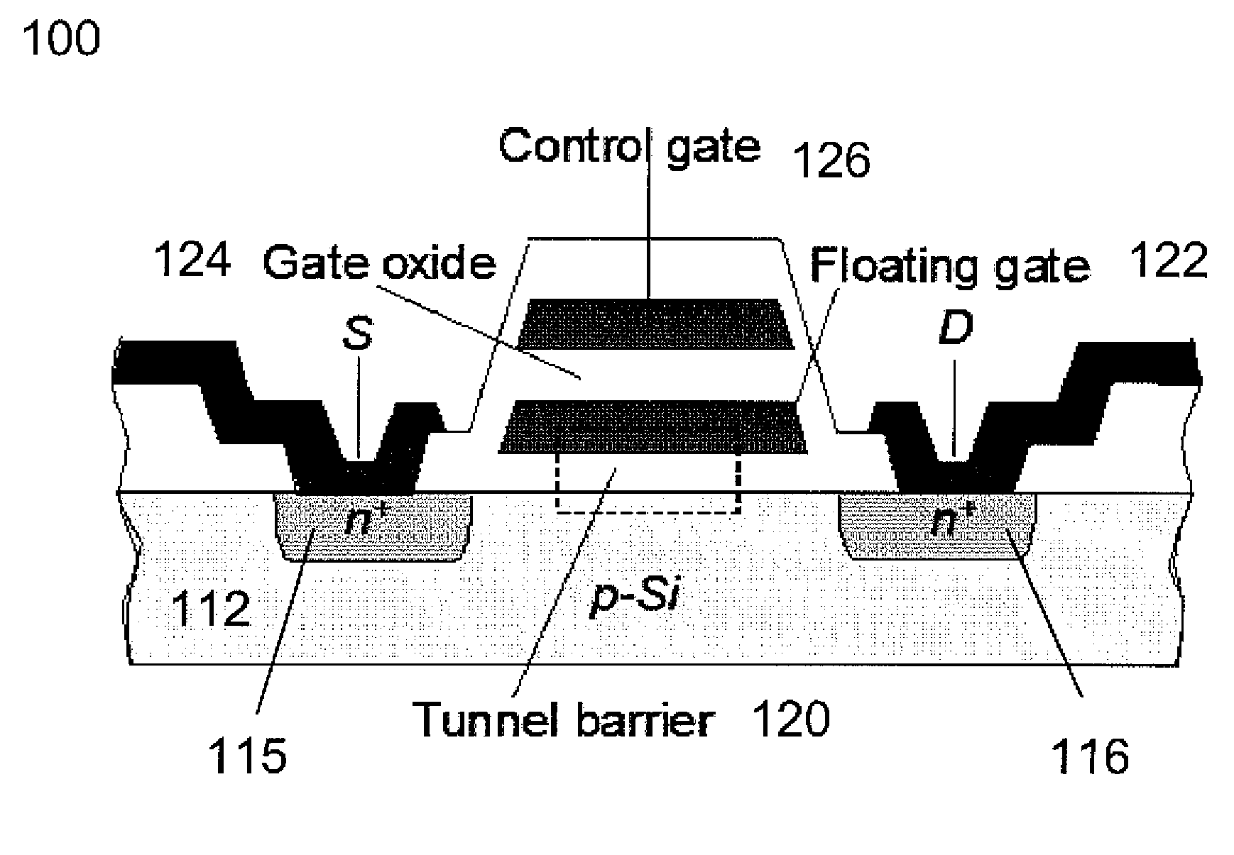
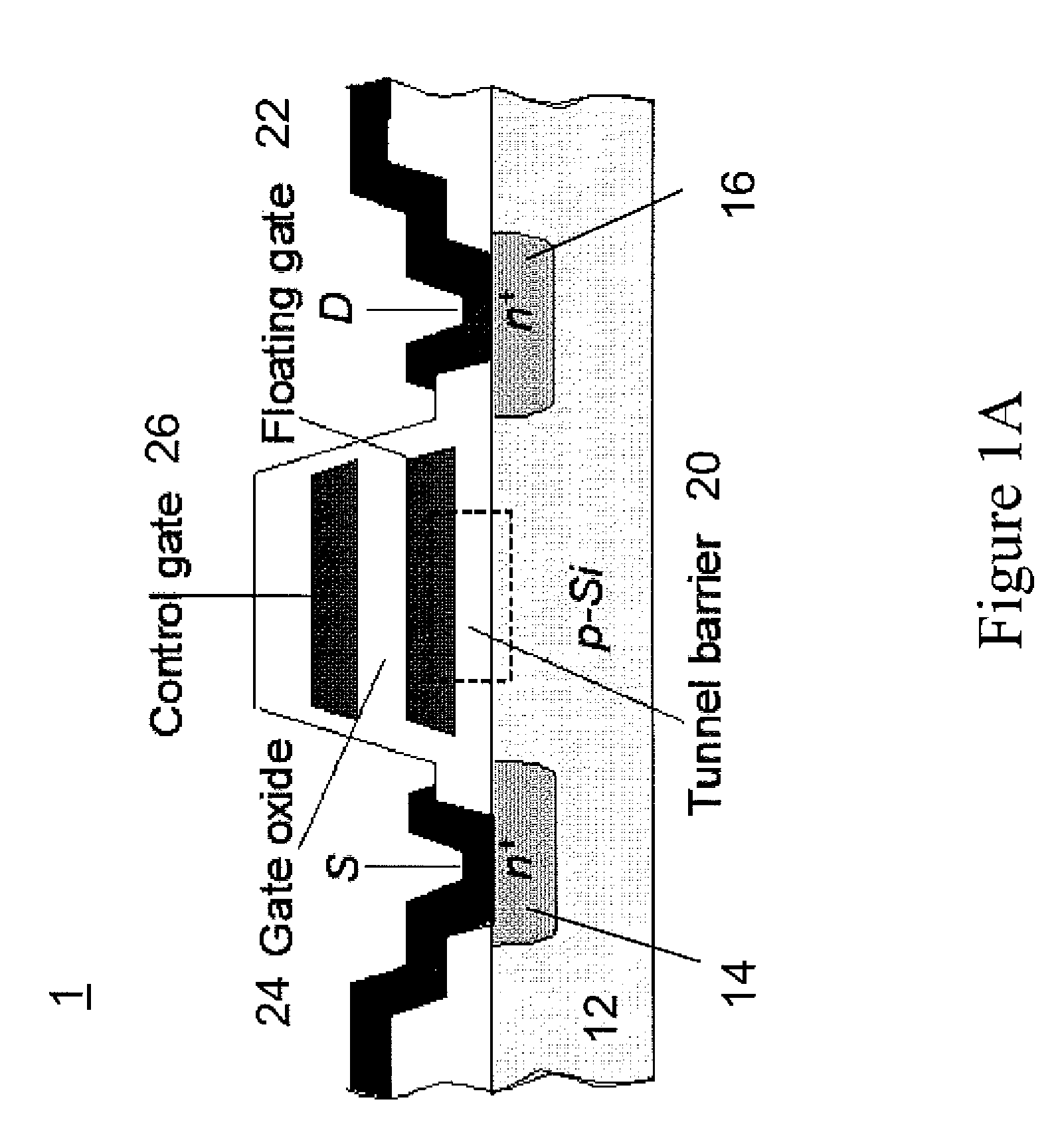
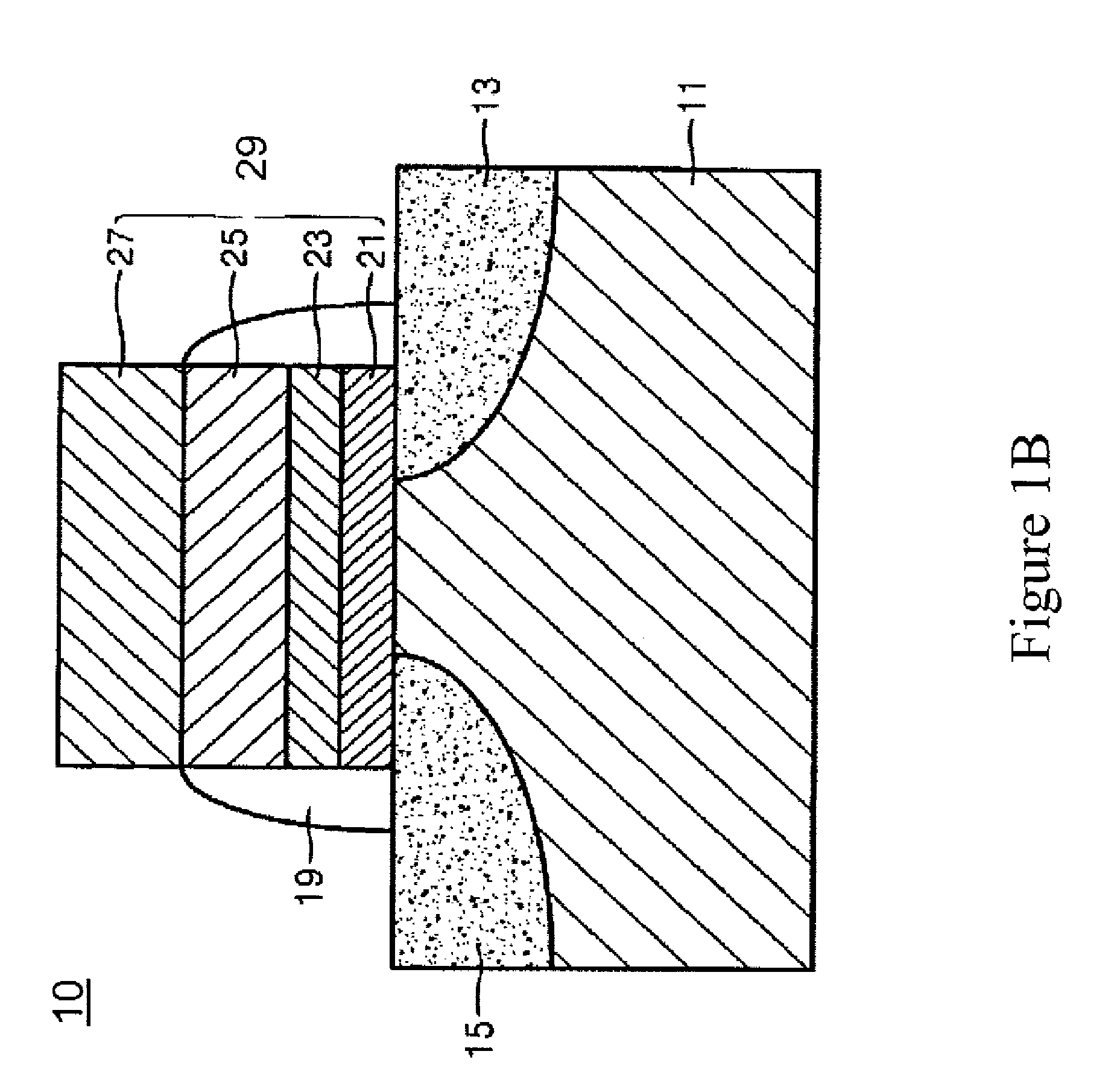
[0034]FIG. 1A shows typical floating gate transistor structures, for example as used in flash memories and other semiconductor devices, showing the gate dielectric. In particular referring to the structure shown in FIG. 1A, the device structure 1 comprises a p type substrate 12, in which is defined source and drain regions 14, 16 and a channel region 18. A first gate oxide layer, i.e. a tunnel dielectric layer 20 is formed on the substrate over the channel region 18 under a floating gate 20, and a second gate oxide 22 or dielectric layer separates the floating gate 20 from a control gate 24. FIG. 1B shows a charge trap type device 10 for a memory cell comprising a substrate 11, source and drain regions 13 and 15, on which is formed a gate structure 29, comprising a tunnel oxide layer 21, a charge trapping layer 23 such as a silicon nitride or oxynitride layer, which may contain semiconductor nanocrystals or other charge trapping material, a charge blocking dielectric layer 25 and a ...


PUM


Abstract

Improved high quality gate dielectrics and methods of preparing such dielectrics are provided. Preferred dielectrics comprise a rare earth doped dielectric such as silicon dioxide or silicon oxynitride. In particular, cerium doped silicon dioxide shows an unexpectedly high charge-to-breakdown QBD, believed to be due to conversion of excess hot electron energy as photons, which reduces deleterious hot electron effects such as creation of traps or other damage. Rare earth doped dielectrics therefore have particular application as gate dielectrics or gate insulators for semiconductor devices such as floating gate MOSFETs, as used in as flash memories, which rely on electron injection and charge transfer and storage.

Description

CROSS-REFERENCE TO RELATED APPLICATIONS[0001]The present invention claims priority from U.S. Provisional Patent Application No. 61 / 187,424 filed Jun. 16, 2009, which is incorporated herein by reference.TECHNICAL FIELD[0002]This invention relates to high quality dielectric materials for semiconductor devices, and in particular to gate dielectrics for semiconductor devices using hot electron injection, e.g. flash memory (EEPROM) and other non-volatile memory devices.BACKGROUND OF THE INVENTION[0003]There are a number of types of semiconductor devices which depend on high quality oxides or dielectrics for reliable operation.[0004]For example, the gate oxide in a conventional MOSFET device or gate dielectric (gate insulator) in an IGFET device or other gate controlled semiconductor device plays a critical role in device performance, reliability and scaling. In such a device, normally no current flows through the gate dielectric, and high quality oxides or dielectrics, with low trap dens...

Claims


Application Information

Patent Timeline
Patent Type & Authority Applications(United States)
IPC IPC(8): H01L29/00H01L29/788H01L21/3115
CPCH01L21/28273H01L29/7881H01L29/51H01L27/11521H01L29/40114H10B41/30
Inventor MINER, CARLAMACELWEE, THOMASALBARGHOUTI, MARWAN
Owner KIRSTEEN MGMT GRP
Why Eureka
Try Eureka