Indium surfactant assisted hvpe of high quality gallium nitride and gallium nitride alloy films

a gallium nitride and alloy film technology, applied in the direction of polycrystalline material growth, crystal growth process, chemically reactive gas growth, etc., can solve the problems of low growth rate of mocvd and mbe techniques, high cost and low volume equipment, etc., to suppress three-dimensional growth, enhance or facilitate two-dimensional growth, and facilitate the epitaxial growth of the film

Inactive Publication Date: 2011-02-03
APPLIED MATERIALS INC
View PDF49 Cites 11 Cited by
  • Summary
  • Abstract
  • Description
  • Claims
  • Application Information

AI Technical Summary

Benefits of technology

[0008]One embodiment of depositing a gallium nitride (GaN) film on a substrate comprises providing a source of indium (In) and gallium (Ga) and depositing a monolayer of indium (In) on the surface of the gallium nitride (GaN) film. The monolayer of indium (In) acts as a surfactant to modify the surface energy and facilitate the epitaxial growth of the film by suppressing three dimensional growth and enhancing or facilitating two dimensional growth. The deposition temperature is kept sufficiently high to enable the indium (In) to undergo absorption and desorption on the gallium nitride (GaN) film without being incorporated into the solid phase gallium nitride (GaN) film. The gallium (Ga) and indium (In) can be provided by a single source or separate sources.

Problems solved by technology

Unfortunately, MOCVD and MBE techniques suffer from low growth rates and the use of expensive, low volume equipment.

Method used


Image

  • Indium surfactant assisted hvpe of high quality gallium nitride and gallium nitride alloy films
  • Indium surfactant assisted hvpe of high quality gallium nitride and gallium nitride alloy films
  • Indium surfactant assisted hvpe of high quality gallium nitride and gallium nitride alloy films

Examples


Embodiment Construction

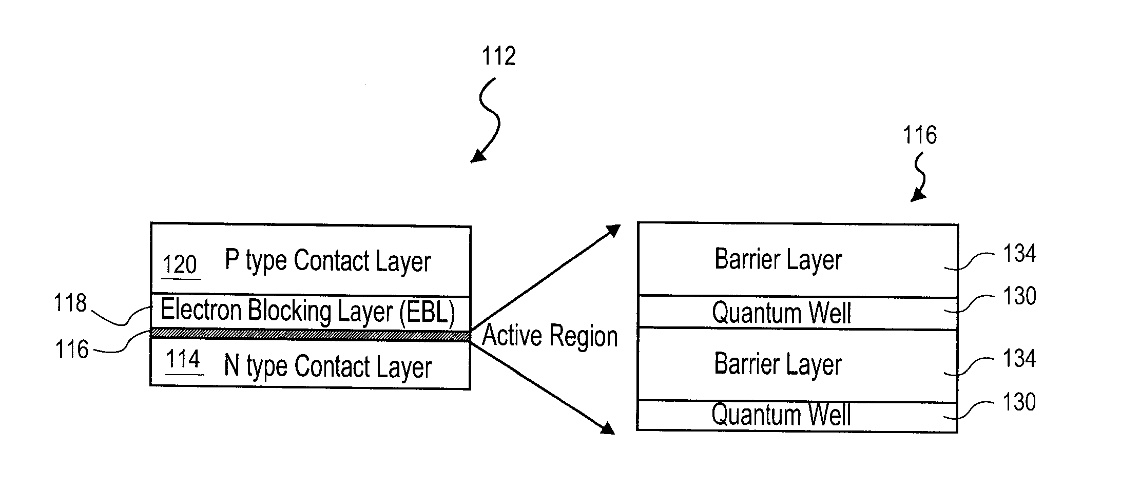
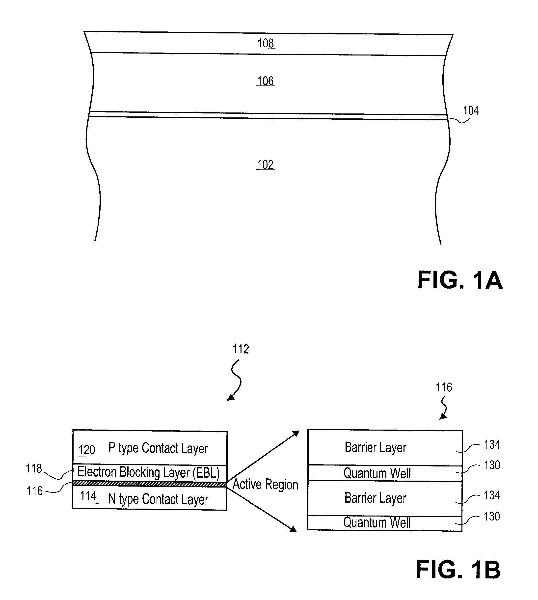
[0020]Embodiments of the present invention describe a method of forming a high quality gallium nitride or gallium nitride alloy epitaxial film utilizing an indium (In) surfactant assisted hydride vapor phase epitaxial (HPVE) deposition process. The present invention has been described with respect to specific details in order to provide a thorough understanding of the invention. One of ordinary skill in the art will appreciate that the invention can be practiced without these specific details. In other instances, well known semiconductor processes and equipment have not been described in specific detail in order to not unnecessarily obscure the present invention.

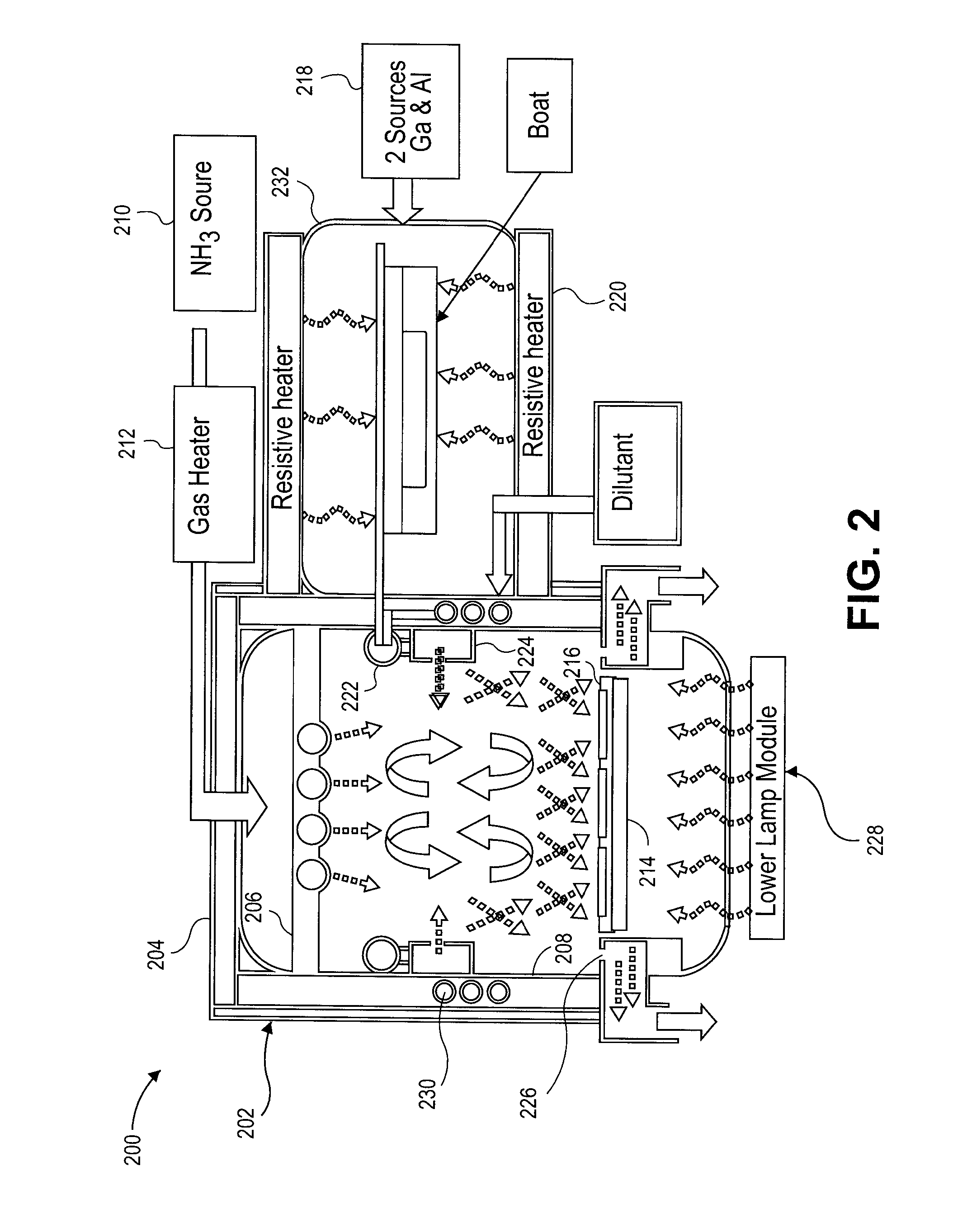
[0021]Embodiments of the present invention describe a method of forming a high quality gallium nitride or gallium nitride alloy epitaxial film utilizing an indium (In) surfactant assisted hydride vapor phase epitaxial (HPVE) deposition process. In an embodiment of the present invention, a small amount of indium, such as betw...


PUM

PropertyMeasurementUnit
deposition temperatureaaaaaaaaaa
thicknessaaaaaaaaaa
thicknessaaaaaaaaaa

Abstract

One embodiment of depositing a gallium nitride (GaN) film on a substrate comprises providing a source of indium (In) and gallium (Ga) and depositing a monolayer of indium (In) on the surface of the gallium nitride (GaN) film. The monolayer of indium (In) acts as a surfactant to modify the surface energy and facilitate the epitaxial growth of the film by suppressing three dimensional growth and enhancing or facilitating two dimensional growth. The deposition temperature is kept sufficiently high to enable the indium (In) to undergo absorption and desorption on the gallium nitride (GaN) film without being incorporated into the solid phase gallium nitride (GaN) film. The gallium (Ga) and indium (In) can be provided by a single source or separate sources.

Description

[0001]This application claims the benefit of and priority to Provisional Application Ser. No. 61 / 230,451, filed Jul. 31, 2009 which is hereby incorporated by reference.BACKGROUND OF THE INVENTION[0002]1. Field of the Invention[0003]Embodiments of the present invention describe method of manufacturing high quality low dislocation density gallium nitride and gallium nitride alloy films, such as aluminum gallium nitride (AlGaN).[0004]2. Discussion of Related Art[0005]Gallium nitride (GaN) and gallium nitride alloy films such as aluminum gallium nitride (AlGaN) films are finding greater importance in the development and fabrication of a variety of semiconductor devices, such as short wavelength light emitting diodes (LEDs), laser diodes (LD) and electronic devices, such as high electron mobility transistors (HEMTs), heterojunction bipolar transistors (HBTs). An important requirement forming these semiconductor devices is the fabrication of a suitable thick gallium nitride layer with a s...

Claims


Application Information

Patent Timeline
Patent Type & Authority Applications(United States)
IPC IPC(8): H01L21/20
CPCC23C16/4488H01L33/06C23C16/45506C30B25/02C30B29/406H01L21/0237H01L21/02458H01L21/02491H01L21/02499H01L21/02502H01L21/0254H01L21/0262H01L29/2003H01L29/7786H01L33/007H01L33/04C23C16/455
Inventor SU, JIEKRYLIOUK, OLGA
Owner APPLIED MATERIALS INC
Why Eureka
Try Eureka