

Thin film transistor
- Summary
- Abstract
- Description
- Claims
- Application Information
AI Technical Summary
Benefits of technology
Problems solved by technology
Method used
Image

Examples
Embodiment Construction
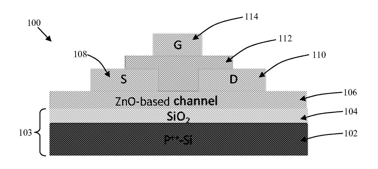
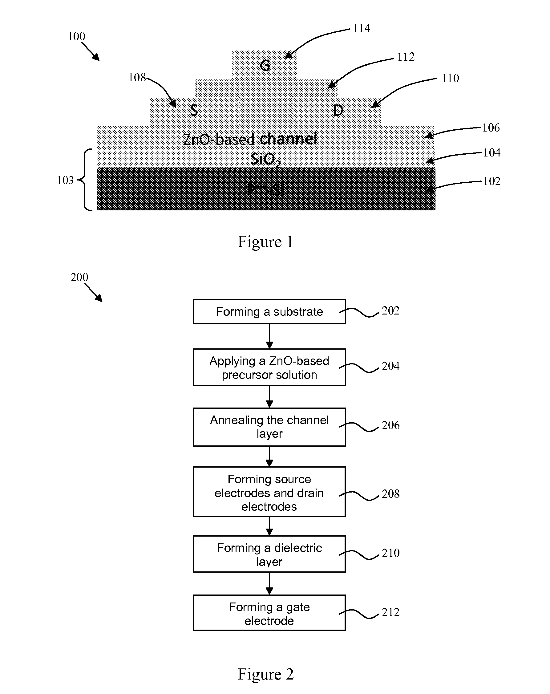
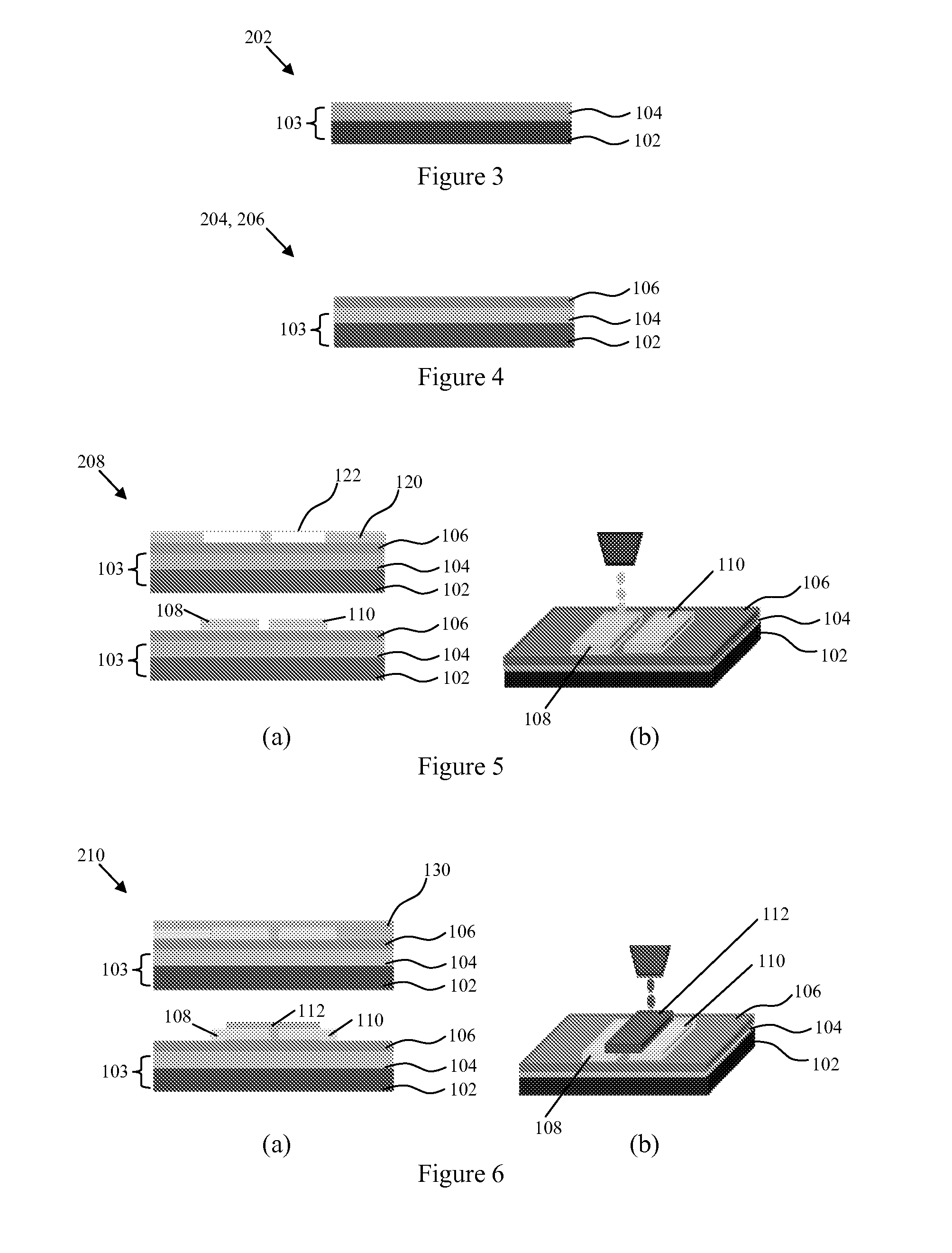
[0027]FIG. 1 shows a dual-gate thin-film transistor (TFT) 100 according to an example embodiment. The TFT 100 comprises a substrate 103 including a highly B-doped Si (p-type) layer 102 and a silicon dioxide (SiO2) layer 104, a zinc oxide (ZnO) based channel layer 106 on the SiO2 layer 104, source 108 and drain 110 electrodes on the channel layer 106, an organic polymer-based dielectric layer 112 on the channel layer 106, and a gate electrode 114 on the dielectric layer 112.
[0028]The p-type layer 102 may have a resistivity of 0.001˜0.006 Ω·cm. Alternatively, this layer may be transparent glass, or polymer substrates that are transparent and flexible. The p-type layer 102 is approximately 500 μm thick. The SiO2 layer 104 is approximately 100 nm thick and functions as a bottom-gate dielectric layer.
[0029]The channel layer 106 may be ZnO, ZnInO, ZnSnO or InSnO and has an amorphous structure. The channel layer 106 may alternative also comprise of a Ga-based oxide. If the channel layer 10...
PUM
 Abstract
Description
Claims
Application Information