Organic Electroluminescent Device

an electroluminescent device and organic technology, applied in the direction of solid-state devices, vacuum evaporation coatings, coatings, etc., can solve the problems of reducing the efficiency of the device, the device cannot escape from the device, and the light may be lost within the device, so as to avoid potential parallax problems, increase the contrast of the electoluminescent device, and enhance the contrast

Active Publication Date: 2011-02-24
CAMBRIDGE DISPLAY TECH LTD
View PDF4 Cites 243 Cited by
  • Summary
  • Abstract
  • Description
  • Claims
  • Application Information

AI Technical Summary

Benefits of technology

[0048]The present inventors have found that the provision of intermediate layers disposed between the substrate and the first electrode all of which have a surface nearest the organic light-emitting layer not more than 150 nm from a surface of the first electrode nearest the organic light-emitting layer results in an increase in out-coupling of light from the device and also improves colour purity. Furthermore, no change in colour with viewing angle is observed.
[0087]According to the second aspect of the present invention there is also provided a method of reducing reflection from a multilayer display device having first and second electrodes, said method comprising: providing anti-reflection means associated with the first electrode; and further providing anti-reflection interference means associated with the second electrode.

Problems solved by technology

A problem with organic electroluminescent devices is that much of the light emitted by organic light-emitting material in the organic light-emitting layer does not escape from the device.
The light may be lost within the device by scattering, internal reflection, waveguiding, absorption and the like.
This results in a reduction in the efficiency of the device.
Furthermore, these optical effects can lead to low image intensity, low image contrast, ghosting and the like resulting in poor image quality.
A further problem with organic electroluminescent devices is that of achieving intense, narrow band-width emission so as to improve the colour purity of emission.
This weak reflectivity of ITO can result in a weak cavity effect.
However, ITO provides a poor cavity not only because it is weak, but also because its refractive index is very variable over the visible spectrum.
One problem with replacing the anode electrode with a stronger mirror is that the electrical properties of the device will be altered.
One problem the present applicant has found with arrangements which utilize a QWS is that the microcavity can be too strong.
Furthermore, the QWS results in a very narrow emission resulting in a narrow viewing angle and the colour of the emission changes with viewing angle.
Additionally, a QWS is complicated and expensive to manufacture requiring the deposition of a number of additional layers and increases the thickness of the finished device.
Another problem the present applicant has found with arrangements which utilize a QWS is that the microcavity can be too large.
One problem with this arrangement is that it is not suitable for improving the colour purity of emission as it is specifically directed to producing a white emission.
Another problem with this arrangement is that, as stated previously, the ITO layer does not form a good cavity.
The above mentioned OLED materials, and in particular the light emitting polymer material and the cathode, are susceptible to oxidation and to moisture.
As a consequence, a problem experienced with prior OLED devices is that the displayed image is degraded by the reflection of ambient light from the cathode 110.
This gives rise to an image that suffers from poorer contrast and worse colour depth than desired.
However, the use of a circular polarizer necessitates increased power consumption and reduces contrast.
Light rays reflected from the two metal layers combine destructively, thereby reducing the amount of reflected ambient light.
There is a desire to reduce the intensity of light reflected from this boundary to the order of 1%, to provide a comparable level of reflection to that which would be achieved by circular polarizers (which, as mentioned above, are disadvantageous in that they necessitate increased power consumption and reduce contrast).
However, this requires adjustment for the effects of thickness, refractive index, etc of the intervening organic layer and as such represents a complex method of minimising reflections at the anode.

Method used


Image

  • Organic Electroluminescent Device
  • Organic Electroluminescent Device
  • Organic Electroluminescent Device

Examples


Embodiment Construction

[0107]Embodiments of the first aspect of the invention will be described first.

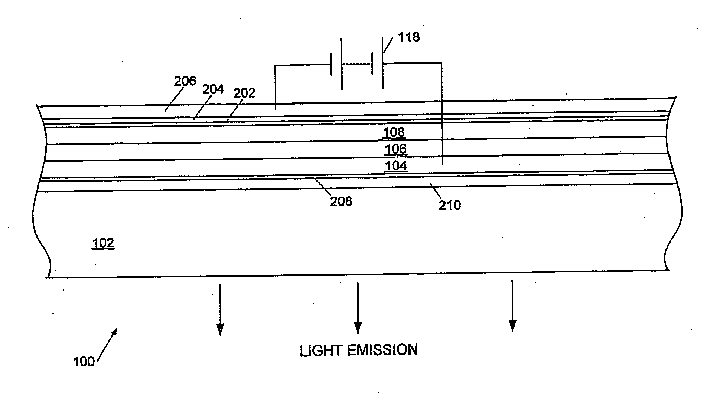
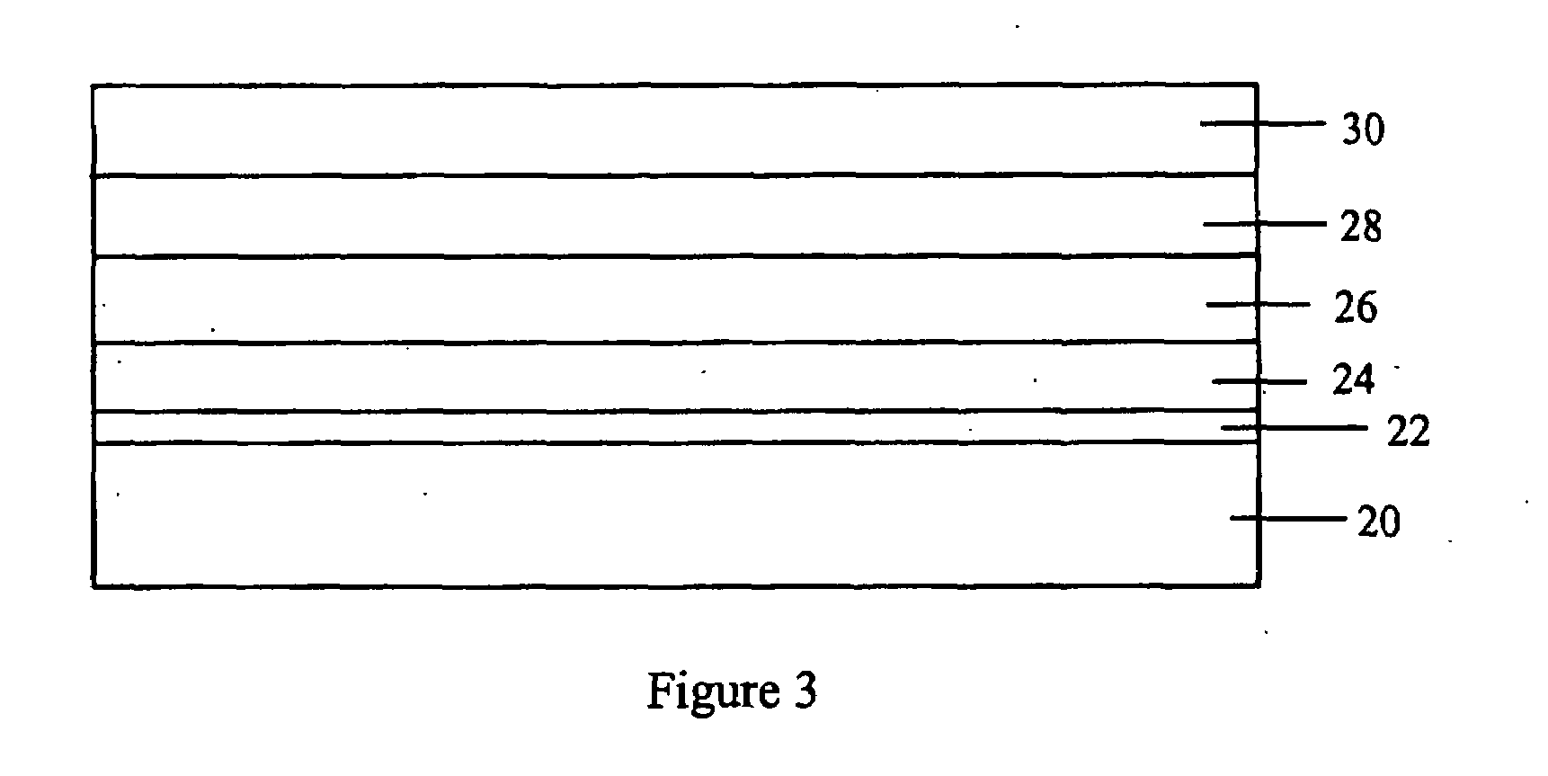
[0108]FIG. 3 shows a bottom-emitting organic electroluminescent device comprising a glass substrate 20, a thin intermediate layer of silver 22 disposed on the glass substrate 20, an anode 24 comprising ITO disposed on the thin silver layer 22, a layer of PEDOT 26 disposed on the ITO 24, a light emitting polymer layer 28 disposed on the PEDOT 26 and a barium / aluminum cathode 30 disposed on the light-emitting polymer layer 28.

[0109]Optical modelling has shown that modifying the anode structure of the polymer light emitting diode structure by including a thin layer of semi-transparent metal improves optical out-coupling and also provides colour tuning of the emission towards the PAL region.

[0110]Modelling has shown that the best materials for the intermediate layer are either high refractive index dielectrics (e.g. titanium dioxide, silicon oxynitride and silicon nitride) or metals that are transparent in th...


PUM

PropertyMeasurementUnit
refractive indexaaaaaaaaaa
wavelengthaaaaaaaaaa
thicknessaaaaaaaaaa

Abstract

An organic electroluminescent device cfomprising: a transparent substrate; a first electrode disposed over the substrate for injecting charge of a first polarity; a second electrode disposed over the first electrode for injecting charge of a second polarity opposite to said first polarity; an organic light-emitting layer disposed between the first and the second electrode, wherein the second electrode is reflective, the first electrode is transparent or semi-transparent, and one or more intermediate layers of dielectric material with a refractive index greater than 1.8 or a metal material is disposed between the substrate and the first electrode forming a semi-transparent mirror whereby a microcavity is provided between the reflective second electrode and the semi-transparent mirror, all the intermediate layers disposed between the substrate and the first electrode having a surface nearest the organic light-emitting layer not more than 150 nm from a surface of the first electrode nearest the organic light-emitting layer.

Description

FIELD OF THE INVENTION[0001]A first aspect of the present invention relates to an organic electroluminescent device. This first aspect also relates to a substrate for an organic electroluminescent device.[0002]A second aspect of the present invention relates to a multilayer display device. It is particularly suitable, but by no means limited, to multilayer display devices fabricated using organic light emitting diodes.BACKGROUND OF THE INVENTION [0003]First Aspect[0004]Organic electroluminescent devices are known, for example from PCT / WO / 13148 and U.S. Pat. No. 4,539,507. Such devices generally comprise a substrate 2, a first electrode 4 disposed over the substrate 2 for injecting charge of a first polarity; a second electrode 6 disposed over the first electrode 4 for injecting charge of a second polarity opposite to said first polarity; an organic light-emitting layer 8 disposed between the first and the second electrodes; and an encapsulant 10 disposed over the second electrode 6....

Claims


Application Information

Patent Timeline
Patent Type & Authority Applications(United States)
IPC IPC(8): H01L51/52H05K1/03H01L51/56B05D5/06C23C14/34
CPCH01L51/5265H01L27/322H10K59/38H10K50/826H10K50/852H10K50/865H01L33/44H01L33/504H01L21/0276H01L2924/12041H10K50/81H10K50/82H10K50/856H10K59/32
Inventor SMITH, EUAN C.QURESHI, FAISALJONGMAN, JAN
Owner CAMBRIDGE DISPLAY TECH LTD
Why Eureka
Try Eureka