CMOS Bandgap Reference Source Circuit with Low Flicker Noises

a reference source circuit and bandgap technology, applied in power conversion systems, instruments, process and machine control, etc., can solve the problems of limited application of cmos bandgap reference circuits, large chips area, and large chips area, so as to reduce the flicker noise resulting from fets and reduce costs. , the effect of low flicker nois

Inactive Publication Date: 2011-02-24
IPGOAL MICROELECTRONICS (SICHUAN) CO LTD
View PDF10 Cites 14 Cited by
  • Summary
  • Abstract
  • Description
  • Claims
  • Application Information

AI Technical Summary

Benefits of technology

The object of the present invention is to furnish a CMOS bandgap reference source circuit with low flicker noise, which uses two overlapping clocks to control the gate of the input FETs of the operational amplifier of the reference circuit, makes the FETs switch alternately between their strong inversion and cut-off regions; consequently, it can effectively reduce the flicker noises resulting from the FETS, cut down the cost, and dispense with special manufacturing techniques.

Problems solved by technology

Two main noise sources with the CMOS bandgap reference result from the flicker noises of field effect transistors (FET) and thermo-noise of all components in circuits.
Consequently, bigger flicker noises have limited the application of the CMOS bandgap reference circuit.
However, this way has led to bigger chips areas, especially when a system requires a reference voltage with lower flicker noises.
However, because the lowpass filter is implemented through resistors and capacitors inside of the chips, it would also cause bigger chips area.
Nevertheless, these methods are relatively complicated, don't fit the mainstream standard of CMOS technology and have increased manufacturing cost as well.

Method used


Image

  • CMOS Bandgap Reference Source Circuit with Low Flicker Noises
  • CMOS Bandgap Reference Source Circuit with Low Flicker Noises
  • CMOS Bandgap Reference Source Circuit with Low Flicker Noises

Examples


Embodiment Construction

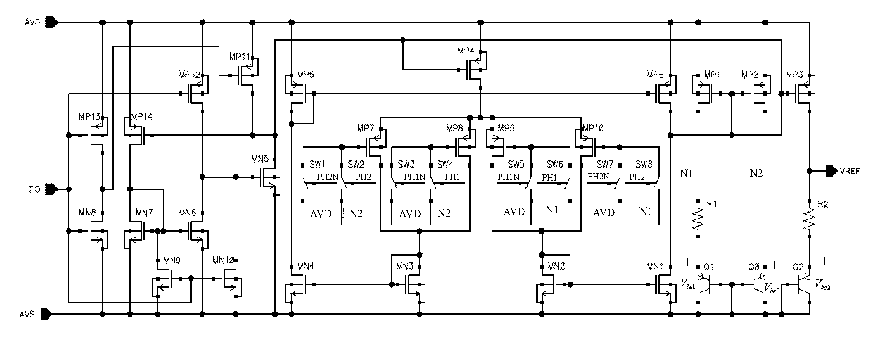
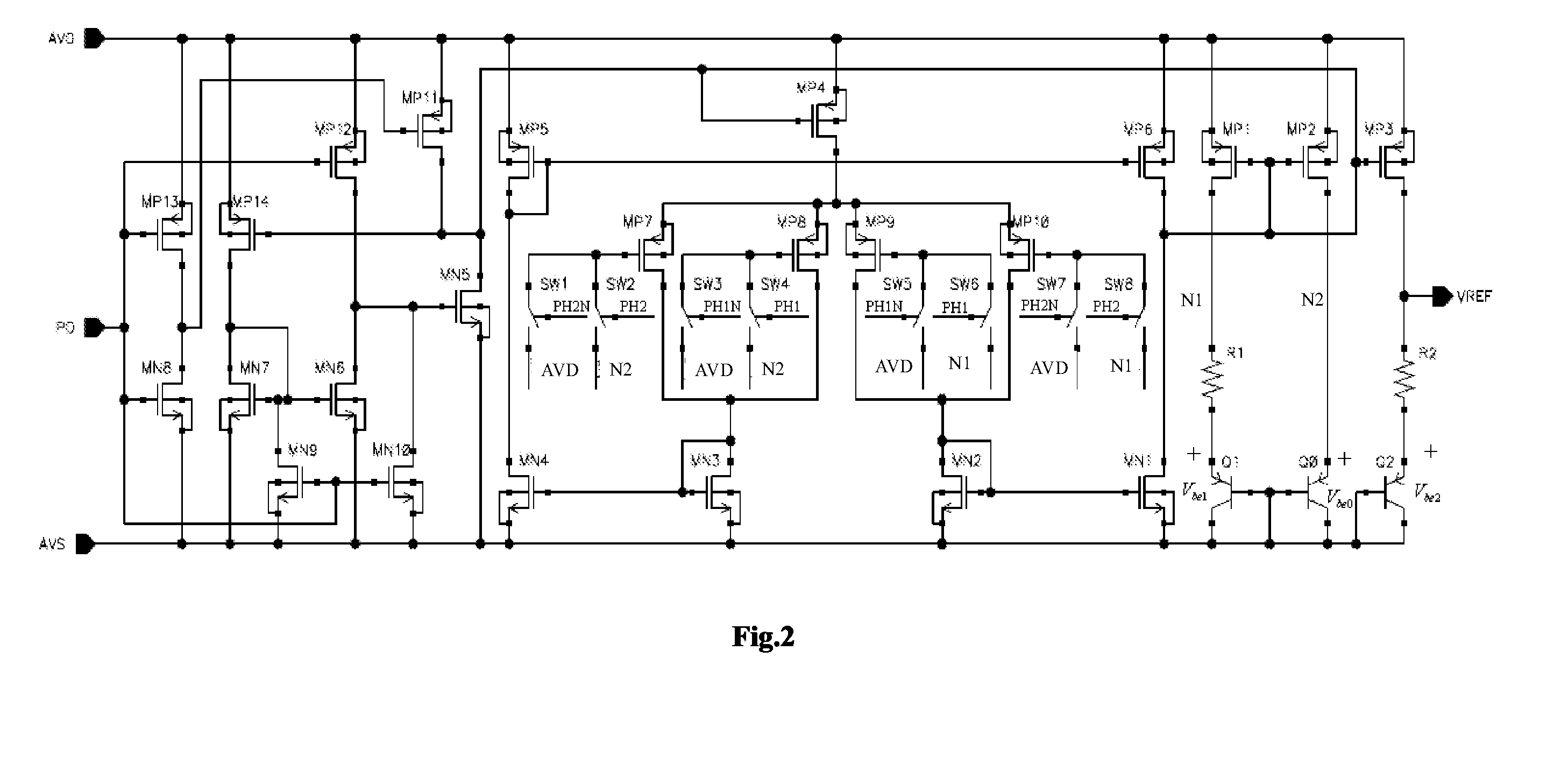
Referring to FIG. 2, a CMOS bandgap reference source circuit with low flicker noises of the present invention comprises a startup circuit, a power-off control circuit, an operational amplifier and a reference voltage generating circuit.

Both the positive and the negative input terminal of the operational amplifier are consisting of two same field effect transistors and both are provided with an input controlled switch. By controlling the input controlled switch, the two FETs in the positive input terminal and two FETs in the negative input terminal work alternately between their strong inversion and cut-off regions, whereby FETs generate very little flicker noises, in turn, the flicker noises resulting from two sets of input transistors of the operational amplifier are reduced drastically.

Said startup circuit comprises of five field effect transistors MP12, MP14, MN5, MN6 and MN7, wherein the width / length ratio of MN6 is far bigger than MN12's. The sources of MP12 and MP14 are connec...


PUM


Abstract

The present abstract discloses a CMOS bandgap reference source circuit, comprising a startup circuit, a power-off control circuit, a reference voltage generating circuit and an operational amplifier. The positive and a negative input terminal of the operational amplifier both consist of two same field effect transistors and both are provided with an input controlled switch; by doing so, two field effect transistors in the positive terminal and two field effect transistors in the negative terminal work alternately between their strong inversion and cut-off region so as to drastically reduce the noises of the reference circuit, which results originally from the flicker noises of two input transistors of the operational amplifier.

Description

BACKGROUND OF THE PRESENT INVENTION1. Field of InventionThe present invention relates to the field of analog integrated circuits and mixed signals integrated circuits, particularly, to a CMOS bandgap reference source circuit with low flicker noises.2. Brief Description of Related ArtsBandgap reference source circuit is an important part of the analog integrated circuit and is widely applied to various analog and mixed signal integrated circuits, such as switching power supply (DC-DC), linear regulator, digital-analog converting circuits (ADC&DAC) and so on, which all need a reference voltage without changing along with the power supply and temperature. Among various reference circuits, the bandgap reference source circuit has better temperature characteristic and power supply rejection ratio (PSRR), is not subject to manufacturing techniques, and accordingly becomes the first option for designing the reference circuit.For some system circuits requiring a reference voltage with high ...

Claims


Application Information

Patent Timeline
Patent Type & Authority Applications(United States)
IPC IPC(8): G05F3/16
CPCG05F3/30
Inventor ZHU, GUOJUN
Owner IPGOAL MICROELECTRONICS (SICHUAN) CO LTD
Why Eureka
Try Eureka