Optical inspection system and method

a technology of optical inspection system and optical inspection method, which is applied in the direction of instruments, electrical appliances, material analysis, etc., can solve the problems of inability to detect small defects on the wafer, difficult to obtain images of all portions of the wafer surface, and difficult to achieve the effect of low throughpu

Active Publication Date: 2011-02-24
NANDA TECH
View PDF28 Cites 18 Cited by
  • Summary
  • Abstract
  • Description
  • Claims
  • Application Information

AI Technical Summary

Benefits of technology

[0006]FIG. 2 illustrates a macro-defect inspection system in which a larger portion including plural dies 3 on a surface of a wafer 1 or the whole wafer surface is imaged onto an image sensor 11. Since a size of available image sensors is typically smaller than a size of the imaged area on the wafer, an imaging optics, schematically indicated at 19, is typically a de-magnifying optics. A dark field light source 21 is provided to generate a dark field illumination beam 22 directed under an acute angle onto the wafer surface such that a main portion of the incident dark field illumination light beam is specularly reflected from the wafer surface to be trapped in a beam dump 23. Defects on the wafer surface, such as small particles or scratches will scatter incident dark field illumination light such that it is collected by the imaging optics 19 and detectable by the image sensor 11. Alternatively or in addition thereto, a bright field light source 25 can be provided to generate a bright field illumination light beam 26 incident onto the wafer surface such that a main portion of the bright field illumination light beam 26 reflected from the wafer surface is also collected by the imaging optics 19 and detected by the image sensor 11. Macro-defect inspection methods as illustrated above with reference to FIG. 2 have the advantage of high throughput since an image of a relatively large portion of the wafer surface can be obtained in a short time, but they have a disadvantage that small defects on the wafer are not detectable due to a limited resolution of available image sensors. Still, macro-defect inspection methods are capable of detecting a large number of possible defects and deficiencies occurring during semiconductor wafer manufacture.
[0041]According to a further exemplary embodiment, the optics provides a dark field illumination beam path including a dark field light source which is mounted to and carried by a second optics carrier which is mounted to and carried by the base. The first and second carriers are commonly mounted on the base but are separate mechanical structures which are not otherwise connected to each other. Such arrangement may have an advantage in that vibrations originating from a cooling system of the dark field light source will not directly induce vibrations of the objective lens and / or the first folding mirror.

Problems solved by technology

Micro-defect inspection methods, such as the one illustrated above with reference to FIG. 1, have the advantage of detecting defects and deficiencies in very small structures of the manufactured semiconductor, but they have the disadvantage of a low throughput, since it will take considerable time to obtain images of all portions of the wafer surface.
Macro-defect inspection methods as illustrated above with reference to FIG. 2 have the advantage of high throughput since an image of a relatively large portion of the wafer surface can be obtained in a short time, but they have a disadvantage that small defects on the wafer are not detectable due to a limited resolution of available image sensors.

Method used


Image

  • Optical inspection system and method
  • Optical inspection system and method
  • Optical inspection system and method

Examples


Embodiment Construction

[0057]In the exemplary embodiments described below, components that are alike in function and structure are designated as far as possible by alike reference numerals. Therefore, to understand the features of the individual components of a specific embodiment, the descriptions of other embodiments and of the summary of the invention should be referred to.

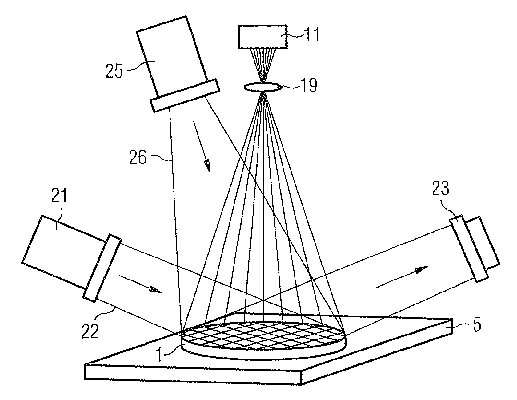
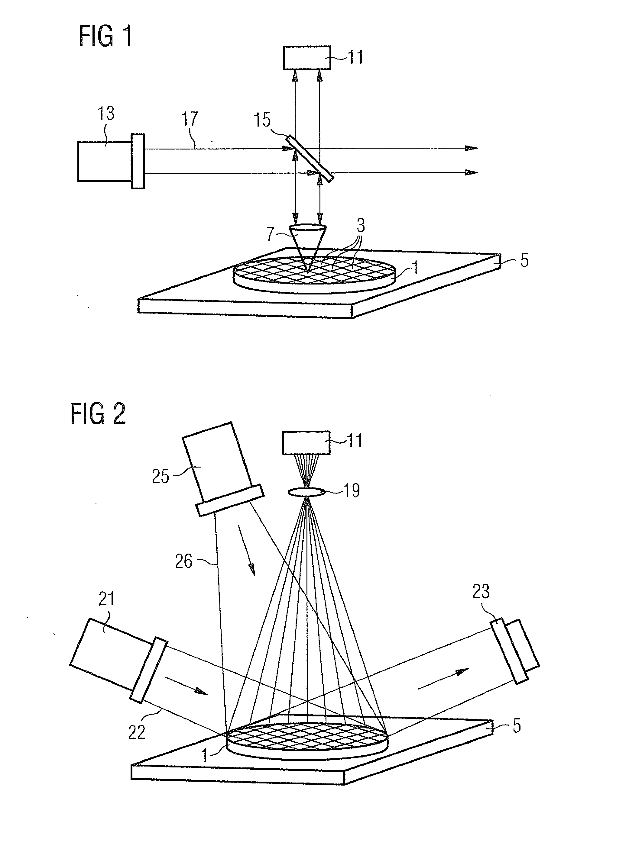
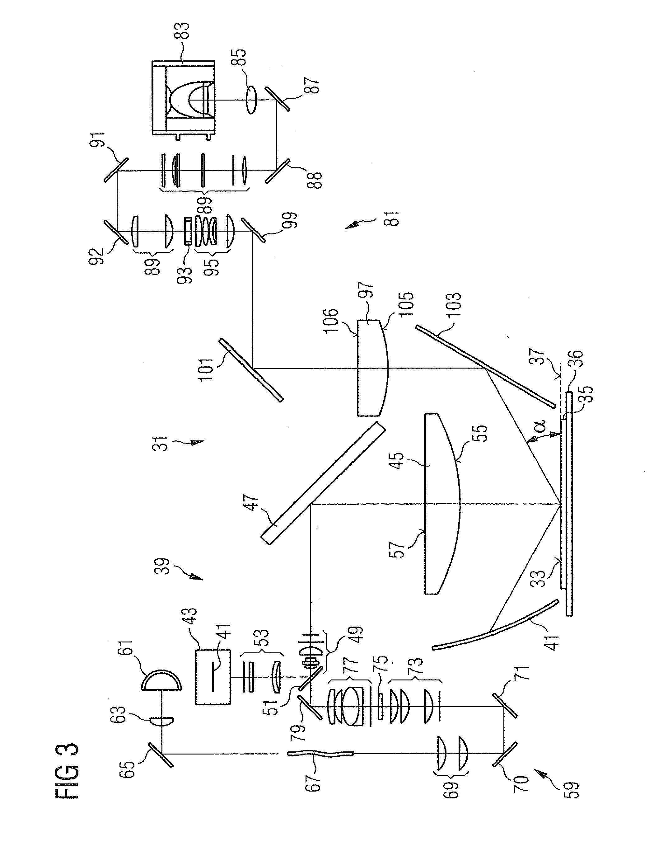
[0058]FIG. 3 is a schematic illustration of a macro-defect inspection system according to an embodiment of the present invention.

[0059]The system 31 is designed to obtain images of surfaces 33 of semiconductor wafers 35. In this embodiment, the wafers 35 are wafers currently used in semiconductor manufacturing having a diameter of about 300 mm. However, the present invention is not limited to such wafer diameters and can be applied to other wafer diameters, such as 400 mm or more which may be used in the future. Moreover, the present invention is generally applicable to inspection of other objects, which may be different from semicon...


PUM

PropertyMeasurementUnit
angleaaaaaaaaaa
angleaaaaaaaaaa
angleaaaaaaaaaa

Abstract

An inspection system includes optics, an object support for mounting an object in a region of an object plane of the optics, a bright-field light source, and a dark-field light source. The inspection system also includes an image detector having a radiation sensitive substrate disposed in a region of an image plane of the optics and a beam dump.

Description

CROSS-REFERENCES TO RELATED APPLICATIONS[0001]This application is a continuation of U.S. application Ser. No. 12 / 715,246, filed Mar. 1, 2010; which claims priority to and is a continuation of International Patent Application No. PCT / EP2009 / 002482, filed Apr. 3, 2009, which claims the benefit of U.S. Provisional Patent Application No. 61 / 064,949, filed Apr. 4, 2008. The disclosures of PCT / EP2009 / 002482 and 61 / 064,949 are hereby incorporated by reference in their entirety for all purposes.BACKGROUND OF THE INVENTION[0002]The present invention relates to optical inspection systems and methods.[0003]Objects of inspection can be generally any types of objects and, in particular, semiconductor wafers. In semiconductor wafer applications, the invention is directed to so-called macro-defect inspection.SUMMARY OF THE INVENTION[0004]Semiconductor circuits are manufactured by forming micropatterned structures on a flat semiconductor wafer substrate using lithographic methods. A wafer substrate...

Claims


Application Information

Patent Timeline
Patent Type & Authority Applications(United States)
IPC IPC(8): G01N21/00
CPCG01N21/9501H01L22/12G01N2021/8825G01N21/956
Inventor MARKWORT, LARSCHHIBBER, RAJESHWARECKERL, KLAUSHARENDT, NORBERT
Owner NANDA TECH
Why Eureka
Try Eureka