Semiconductor device with acene heat spreader

Inactive Publication Date: 2011-03-03
HITACHI LTD
View PDF3 Cites 8 Cited by
  • Summary
  • Abstract
  • Description
  • Claims
  • Application Information

AI Technical Summary

Benefits of technology

[0007]More specifically, (1) in a semiconductor device having a semiconductor chip, a plurality of leads electrically connected to the semiconductor chip and mainly made of metal and a sealing body for sealing the semiconductor chip, it is effective that a material having acene as a matrix organic matter is used for the sealing body.
[0013]According to the present invention, it is possible to provide a semiconductor device with improved heat dissipation characteristics capable of preventing the occurrence of the failure. Further, a semiconductor device with high reliability can be provided and a manufacturing method of a semiconductor device with high yield can be provided.

Problems solved by technology

In such a circumstance, since the heat generation density of a chip has been increasing, it has become impossible to ensure the sufficient heat dissipation characteristics even when the sealing body in which a thermosetting resin with a high heat conductivity is used as matrix and an inorganic ceramics powder is used as filler (filling material) as described in the Patent Document 2 (Japanese Patent Application Laid-Open Publication No. 2003-282798) is used.

Method used


Image

  • Semiconductor device with acene heat spreader
  • Semiconductor device with acene heat spreader
  • Semiconductor device with acene heat spreader

Examples


first embodiment

[0036]Hereinafter, an embodiment of the present invention will be described in detail based on the examples shown in the accompanying drawings.

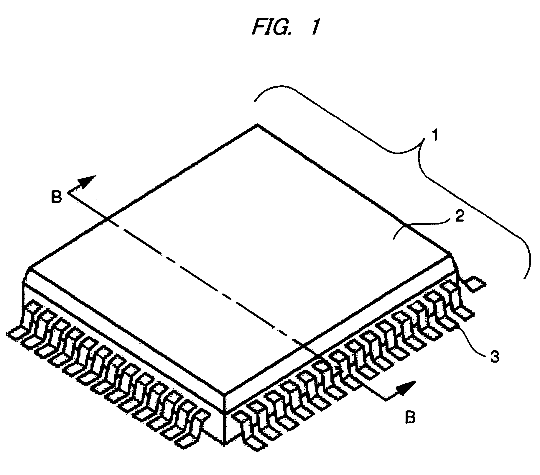
[0037]First, FIG. 1 shows a perspective view of a semiconductor device according to the first embodiment of the present invention. Also, FIG. 2 shows a cross-sectional view taken along the line A-B in FIG. 1. The package type of the semiconductor device according to the present embodiment is QFP (Quad Flat Package).

[0038]As shown in FIG. 1, a semiconductor device 1 according to the first embodiment is covered with a sealing body 2 having an organic matter as a matrix material, and leads 3 are protruded from four side surfaces of the sealing body 2. The lead 3 has a structure bent into an L shape.

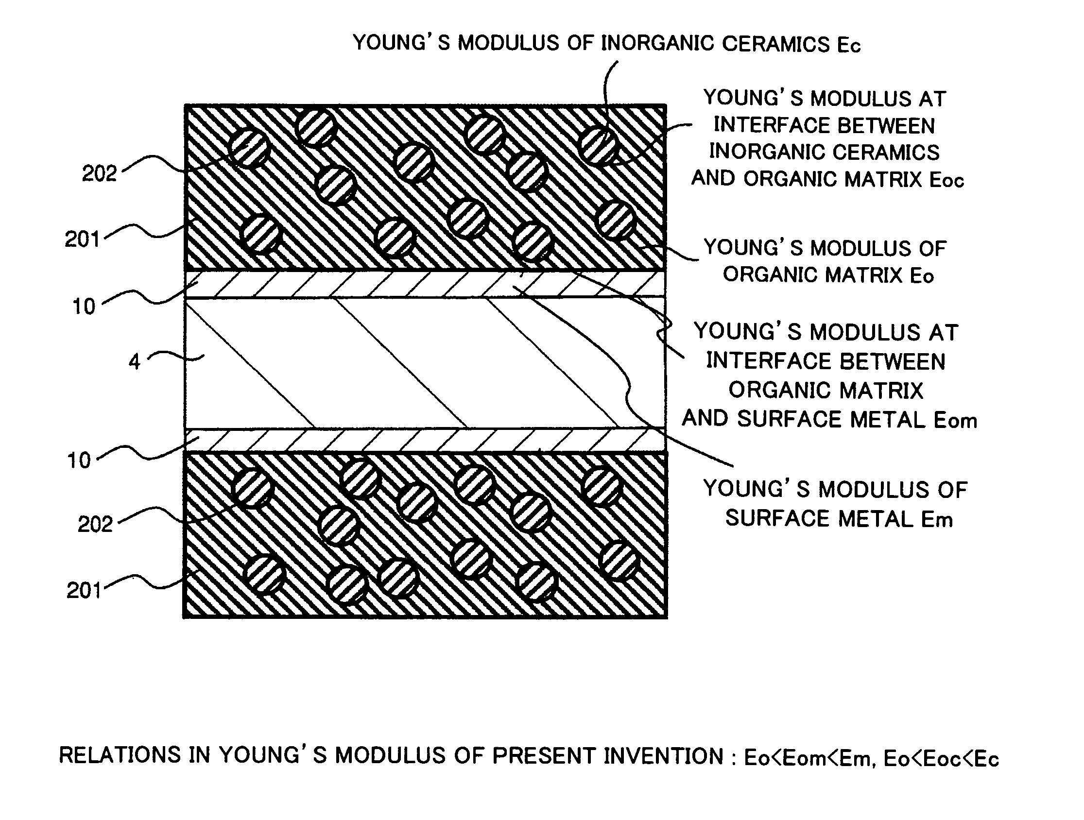
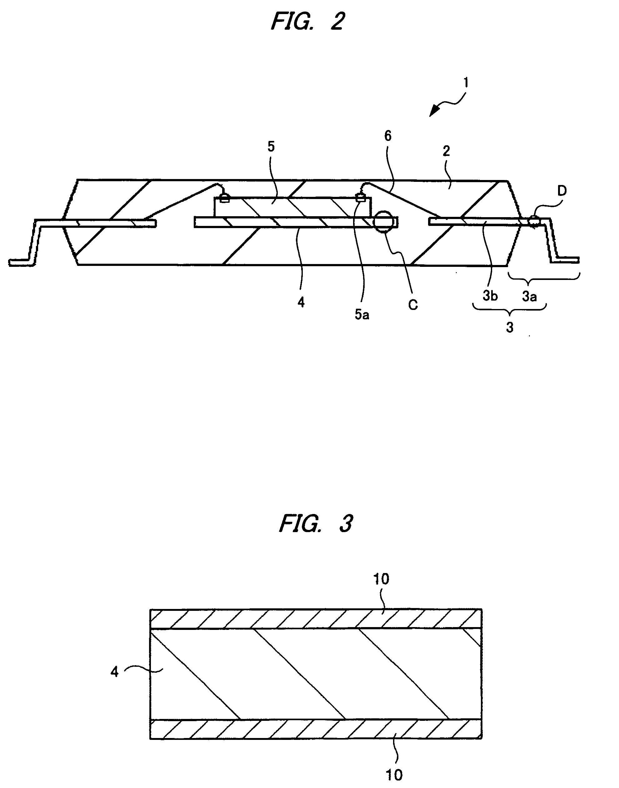
[0039]Also, as shown in FIG. 2, the lead 3 is made up of an outer lead 3a protruded from the side surface of the sealing body 2 and an inner lead 3b formed inside the sealing body 2. In a central portion sandwiched by left and right inner leads 3b (su...


PUM


Abstract

A semiconductor device in which an adhesion between a lead and a sealing body (mold sealing body) is improved to prevent the peering is provided. In a semiconductor device having a semiconductor chip, a plurality of leads electrically connected to the semiconductor chip and mainly made of metal and a sealing body for sealing the semiconductor chip, in order to improve the adhesion between the lead and the sealing body (mold sealing body), a material combination with good lattice matching is used as a combination of a surface material of the lead and a material of the sealing body, and the sealing body mainly made of acene is used.

Description

CROSS-REFERENCE TO RELATED APPLICATION[0001]The present application claims priority from Japanese Patent Application No. 2009-199189 filed on Aug. 31, 2009, the content of which is hereby incorporated by reference to this application.TECHNICAL FIELD OF THE INVENTION[0002]The present invention relates to a semiconductor device and a manufacturing technology thereof, and more particularly to a technology effectively applied to a semiconductor device having a structure in which an organic matter is used as a sealing body for sealing a semiconductor chip and to its manufacture.BACKGROUND OF THE INVENTION[0003]Japanese Patent Application Laid-Open Publication No. 9-195068 (Patent Document 1) discloses a method in which, after Cu strike plating is performed to a lead base material made of Cu alloy as base plating, silver, gold, palladium and others for wire bonding or die bonding are partially plated, and then a semiconductor chip having leads connected thereto is sealed with a sealing bo...

Claims


Application Information

Patent Timeline
IPC IPC(8): H01L23/495H01L21/50
CPCH01L23/295H01L23/49568H01L2924/01068H01L2924/01055H01L2924/12044H01L2924/01079H01L2924/01078H01L2924/01046H01L2924/01029H01L23/49582H01L23/49586H01L24/48H01L2224/48091H01L2224/48247H01L2224/48465H01L2924/01013H01L2924/00014H01L2924/00H01L2924/14H01L2924/181H01L2924/00012H01L2224/45099H01L2224/45015H01L2924/207
Inventor IWASAKI, TOMIO
Owner HITACHI LTD
Why Eureka
Try Eureka