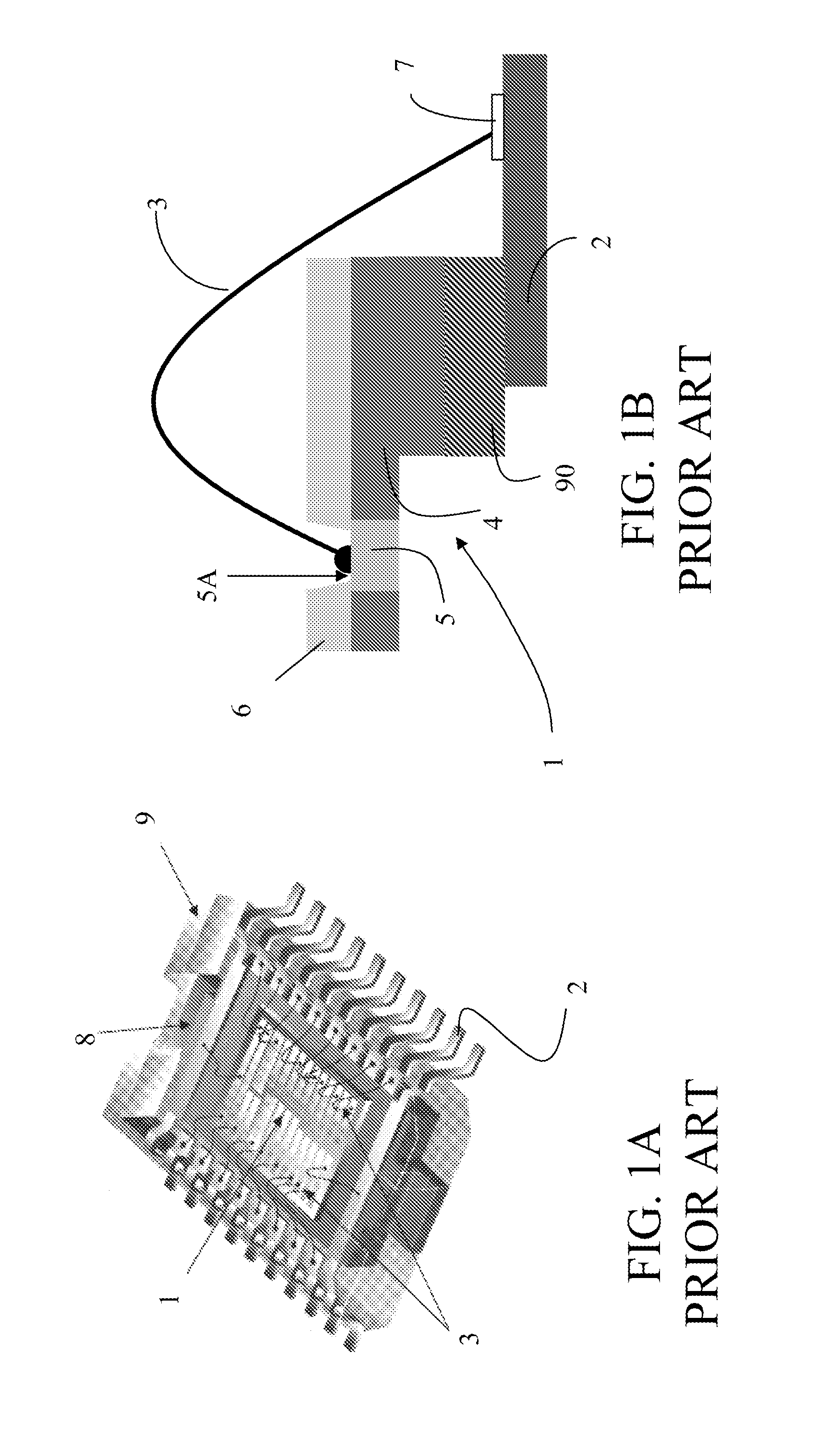
The use of probes that are positioned on the pads to electrically connect the tester to the wafer implies a damaging of the
metal the pads are made of, creating big problems, not only during the testing or “probing”, but especially during the assembly of the die.
If the probes of a
probe card are placed on the pad 5, this latter can be damaged.
In particular, this damaging of the surface of the pad can imply a poor adhesion of the bonding metallic wire to the damaged surface, causing the detachment of the wire from the pad, or even a total lack of adhesion and, thus, the impossibility of creating an electric connection through
wire bonding.
A further problem arises, when more dice should be embedded inside a package in “stacked” configurations for example of the pyramidal (pyramidal stacked), symmetrical (twin stacked), or with rotated overlapping (overhanging stacked) types, which consist in stacking different dice of different size one above the other, and then creating the connections between the dice and between die and support element of the package through
wire bonding.
In fact, in this type of configuration it often occurs that the sizes of the upper die are limited to the position of the pads and of the corresponding
wire bonding of the die.
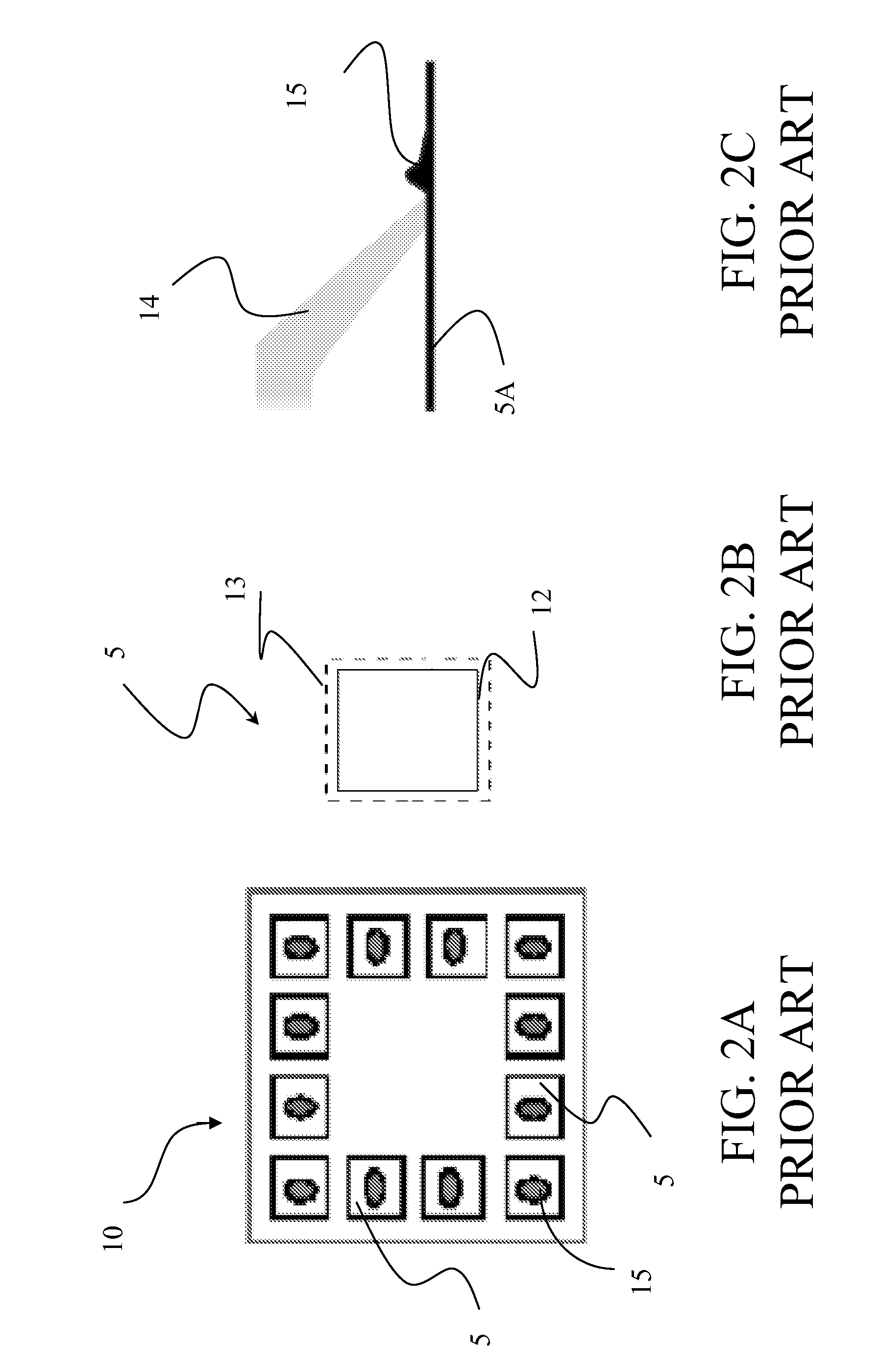
A further problem arises during the performance of a testing of more devices in parallel, for which probe cards with a very high number of probes may be used.
This determines an increase of the contacting problems and, thus, of electrical continuity, between the
probe card and the wafer, i.e., between the probes and pads of the device to be tested, which causes successive probing on the same devices.
Although the Studded Pad is advantageous in terms of protection of the
layers underlying the pad, to form the protection
oxide grid of the
copper metallization layer, additional process steps are involved, which consequently burden and complicate the manufacturing of the device.
A further problem of the performance of a probing through probes is represented by the mechanical limits of the devices of last generation, which have a high number of pads to be contacted or pads with reduced area or also pads very close to each other, i.e., with reduced “
pitch” or “
fine pitch”.
In fact, in case of pads with
reduced size and of a high temperature of the wafer, for example much higher than 25 degrees centigrade, it can occur that at least one probe of the
probe card, after having contacted the pad, moves on the pad itself due to the
thermal expansion of the probe card, causing the breakage of the passivation layer surrounding the pad with a subsequent loss of electric yield.
However, the probes being placed also on the primary pads inside the area of the device, this known solution shows the same probe damaging problems previously discussed.
Although advantageous under several aspects, this known solution shows the main
disadvantage of not allowing to simultaneously test two adjacent chips, since it involves skipping at least one
chip.
Moreover, the manufacturing process of the devices is complicated by the fact that additional process steps are used to realize the POP and create the additional metallization layer above the passivation layer.
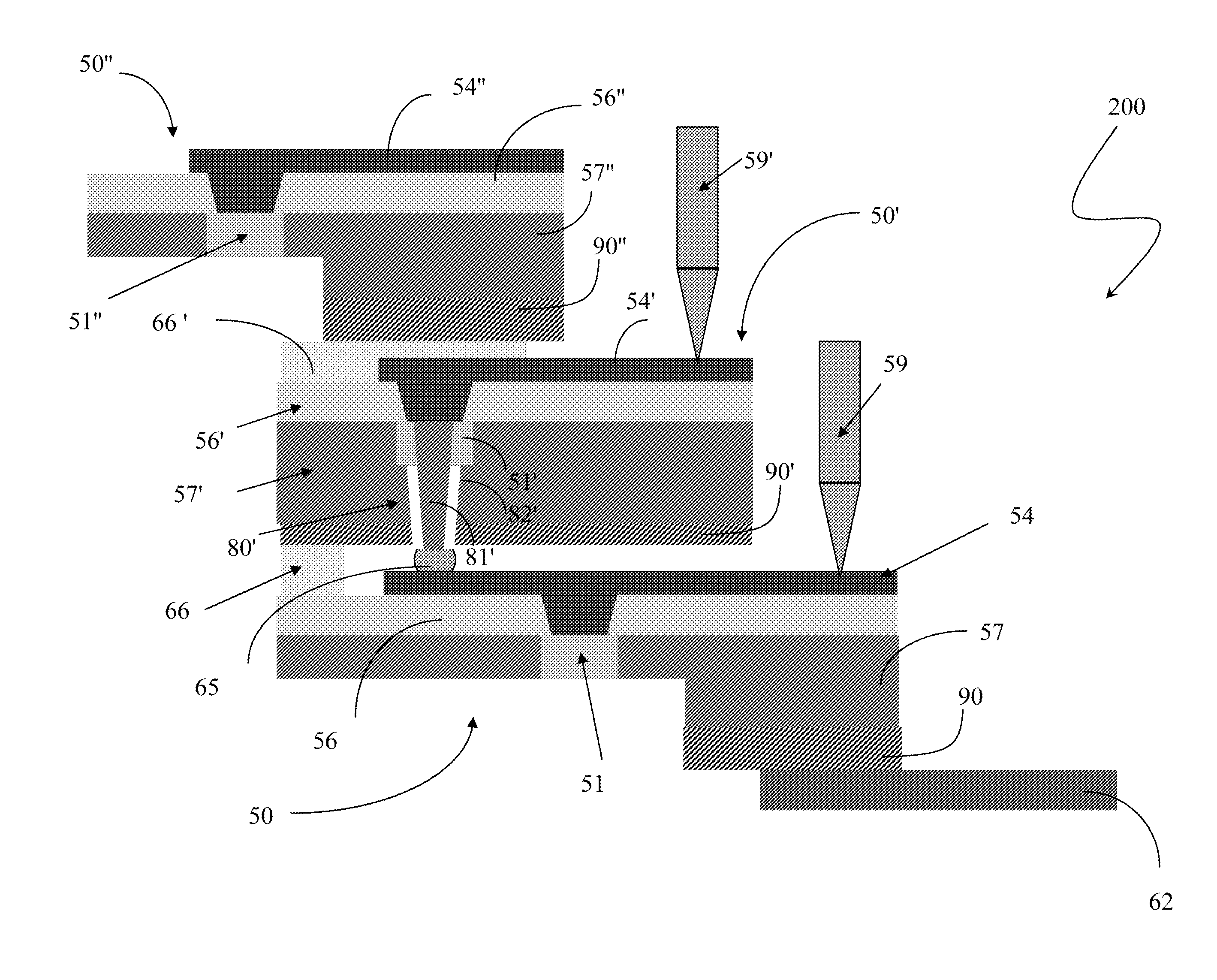
The problems relative to the probing and to the successive step in which the electric connections to the
chip are created, are mainly shown when the electrical testing is to be performed on wafers comprising devices with conductive bumps above the pads.
In particular, further to one or more probing the bump is damaged in different areas of its area useful to perform the successive assembly and to create the electric connection.
Therefore, the formation of electric connections can result remarkably jeopardized.
Moreover, the performance of the probing on bump is more problematic with respect to that of the probing on pad, since the bumps can show different heights with respect to one another and can be realized with also non planar geometries.
And in the structures that show both the pad and the bump, the use of the probes for the probing often creates a damage on both.
However, the creation of a
redistribution layer implies additional process steps, that burden the assembly process, indeed.

