Magnetic memory element, method of driving same, and nonvolatile storage device

a technology of magnetic memory element and magnetic memory element, which is applied in the direction of digital storage, galvano-magnetic material selection, instruments, etc., to achieve the effects of high integration level, low cost and high performance non-volatil

Active Publication Date: 2011-03-17
III HLDG 3
View PDF5 Cites 36 Cited by
  • Summary
  • Abstract
  • Description
  • Claims
  • Application Information

AI Technical Summary

Benefits of technology

[0014]In a magnetic memory element of this invention, it is preferable that the magnetic compensation temperature Tcomp of the N-type ferrimagnetic material be lower than the temperature reached by the ferrimagnetic layer when one write pulse is applied, and higher than the temperature reached by the ferrimagnetic layer when another write pulse is applied. That is, it is preferable that write pulses such that the temperature of a ferrimagnetic layer having the N-type ferrimagnetic material does not become higher than the magnetic compensation temperature Tcomp, and write pulses such that the magnetic compensation temperature Tcomp is exceeded, be used selectively. By this means, writing is performed in a state in which the apparent magnetization of the ferrimagnetic layer is directed in a desired direction. In this way, the magnetization combination can be controlled using a simple structure. Also, switching by current-induced magnetization reversal is possible using single-polarity electric pulses. Here, as write pulses, when writing information as a state of a combination of the magnetization of the free layer and the magnetization of the pinned layer, two pulses can be used so as to write a state of combination of two magnetizations according to two different information elements. According to these write pulses, current-induced magnetization reversal can be induced so as to erase the immediately preceding state if necessary, and the desired magnetization combination state can be realized and used for information recording.
[0042]In a nonvolatile storage device comprising a magnetic memory element and a method of driving such an element of this invention, as explained above, switching can be performed using single-polarity electric pulses, so that a one diode-one MTJ, 4 F2 size memory cell can be configured. As a result, a high-speed nonvolatile storage device with high integration levels can be realized at low cost.

Problems solved by technology

Further, as a separate mode, the layer thickness of the pinned layer may be made sufficiently large, so that changes in the magnetization do not readily occur, and the magnetic characteristics of the pinned layer may be made different from those of the free layer.

Method used


Image

  • Magnetic memory element, method of driving same, and nonvolatile storage device
  • Magnetic memory element, method of driving same, and nonvolatile storage device
  • Magnetic memory element, method of driving same, and nonvolatile storage device

Examples


second embodiment

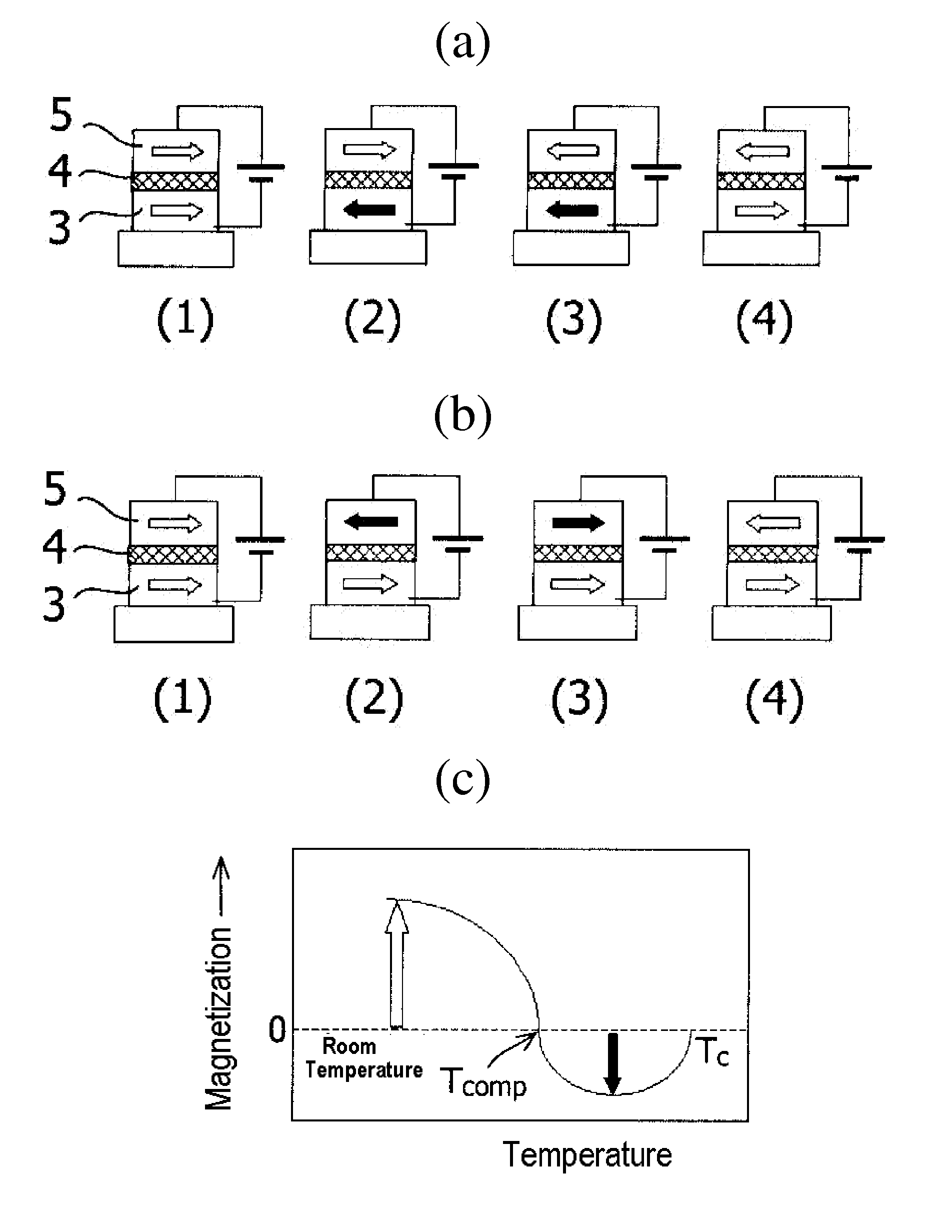
[0073]Next, an example of the configuration of a nonvolatile storage device (device of this invention), using elements of this invention as memory cells, is explained using FIG. 10 and FIG. 11.

[0074]FIG. 10 schematically shows a magnetic memory element and a rectifying element comprised by a cross-point type memory cell array, which is a practical example of a nonvolatile storage device of this invention. As already explained, by means of a magnetic memory element and a method of driving such an element of this invention, switching using single-polarity electric pulses is possible. A rectifying element (here, an example of a diode is shown) is connected in series as a selection switch for the element, and by forming upper electrodes and lower electrodes in an array shape, a cross-point type memory is formed. For example, diodes can be formed in advance on a Si substrate, and magnetic memory elements of this invention can then be formed thereabove. By applying positive-polarity elect...


PUM


Abstract

In order to obtain a memory cell of size 4 F2 to realize cross-point type memory, a magnetic memory element is used having a spin valve structure including a free layer 5, nonmagnetic layer 4, and layer 3. The layer or the free layer includes an N-type ferrimagnetic material, and the magnetic compensation point of the N-type ferrimagnetic material is lower than the temperature reached by the layer when a certain write pulse is applied to control the combination of magnetizations of the free layer and layer, and higher than the temperature reached by the layer when another write pulse is applied. These write pulses can have the same polarity.

Description

TECHNICAL FIELD[0001]This invention relates to a magnetic memory element capable of storing information by electrical means, a method of driving such an element, and a nonvolatile storage device.BACKGROUND ART[0002]In recent years the increase in capacity of nonvolatile semiconductor storage devices, of which flash memory is representative, has been remarkable, and there have been announcements of the release of products with capacities of approximately 32 Gbytes. In particular, the commodity value as USB memory and as storage for mobile phones is increasing. That is, nonvolatile semiconductor storage devices exploit the inherent superiority of solid-state memory devices as storage for portable music players, with respect to resistance to vibrations, high reliability, and low power consumption, so that such devices are becoming the mainstream of storage for the above mobile or portable music or video commercial products.[0003]On the other hand, separately from the above-described st...

Claims


Application Information

Patent Timeline
Patent Type & Authority Applications(United States)
IPC IPC(8): G11C11/02G11C11/06
CPCG11C11/16H01L43/10H01L27/224G11C11/1659G11C11/161G11C11/1675H10B61/10H10N50/85H10N50/10H10N50/01
Inventor OGIMOTO, YASUSHI
Owner III HLDG 3
Why Eureka
Try Eureka