Patterning Method for Carbon-Based Substrate

a technology of carbon-based substrates and substrates, which is applied in the direction of decorative surface effects, nanotechnology, material nanotechnology, etc., can solve the problems of difficult reduction of the manufacturing cost of carbon-based substrates, complex and time-consuming manufacturing process, and inability to widely use carbon-based substrates in various electronic products

Inactive Publication Date: 2011-03-31
IND TECH RES INST
View PDF12 Cites 21 Cited by
  • Summary
  • Abstract
  • Description
  • Claims
  • Application Information

AI Technical Summary

Benefits of technology

[0006]The invention is directed to a patterning method for a carbon-based substrate. The carbon-based substrate is etched by an oxygen-contained plasma at an atmospheric pressure, so that the process of patterning the carbon-based substrate is more efficient and more convenient.

Problems solved by technology

However, the strong anti-corrosion of the carbon-based substrate makes the manufacturing process thereof complicated and time-consuming.
Thus, the manufacturing cost of the carbon-based substrate is hard to be reduced and the carbon-based substrate cannot be widely used in various electronic products.

Method used


Image

  • Patterning Method for Carbon-Based Substrate
  • Patterning Method for Carbon-Based Substrate
  • Patterning Method for Carbon-Based Substrate

Examples


Embodiment Construction

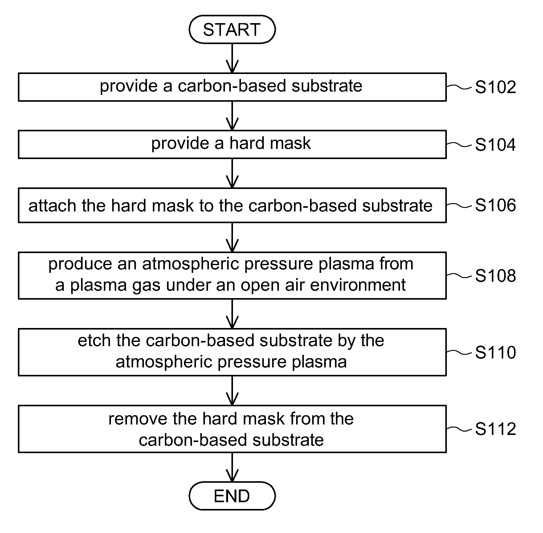
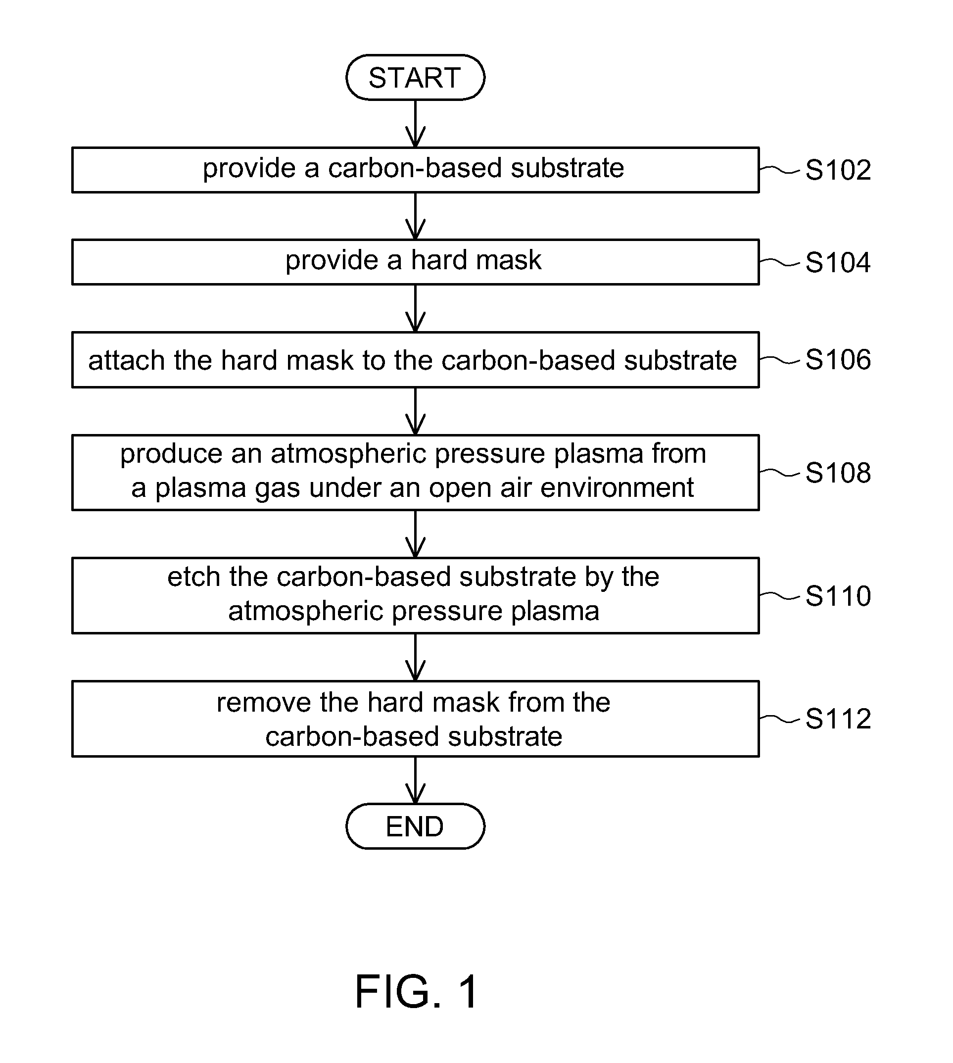
[0011]The invention is exemplified by an embodiment below. However, the embodiment is for exemplification only, not for limiting the scope of protection of the invention. Besides, secondary elements are omitted in the embodiment for highlighting the technical features of the invention.

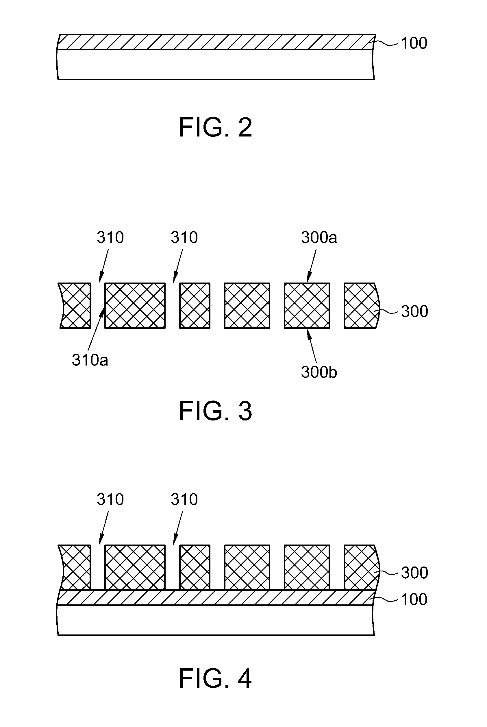
[0012]Referring to FIG. 1 and FIGS. 2-7. FIG. 1 shows a flowchart of a patterning method for a carbon-based substrate 100. FIGS. 2-7 show the respective steps of FIG. 1.

[0013]Firstly, the method begins at step S102, as indicated in FIG. 2, a carbon-based substrate 100 is provided. In the present embodiment of the invention, the carbon-based substrate 100 is exemplified by a transparent carbon nanostructure-based thin film like carbon nanotube or nano-graphite. The optical properties of the transparent carbon nanostructure-based thin film are similar to that of the indium tin oxide film (ITO film). The transparent carbon nanostructure-based thin film having high electron conductivity can be used to form...


PUM

PropertyMeasurementUnit
transmittanceaaaaaaaaaa
atmospheric pressureaaaaaaaaaa
transparentaaaaaaaaaa

Abstract

A patterning method for a carbon-based substrate is provided. The patterning method for the carbon-based substrate includes the following steps. The carbon-based substrate is provided. An atmospheric pressure plasma is produced from a plasma gas under an open air environment. The plasma gas includes oxygen. The carbon-based substrate is etched by the atmospheric pressure plasma.

Description

BACKGROUND OF THE INVENTION[0001]1. Field of the Invention[0002]The invention relates in general to a patterning method for a substrate, and more particularly to a patterning method for a carbon-based substrate.[0003]2. Description of the Related Art[0004]The carbon-based substrate, having the features of high conductive, high strength and high bendability, has attracted great attention in recent years. The multi-touch effect can be achieved if a circuit pattern like a transistor array is marked on the carbon-based substrate so as to form a transparent carbon nanostructure-based thin film. The transparent carbon nanostructure-based thin film, having achieved the standards of 85% transmittance and 200 Ω / sq impedance, can be used in the touch panel of various electronic products.[0005]The traditional IC processes use a photo resistor in a lithography step and a wet etching step to form the circuit pattern. However, the strong anti-corrosion of the carbon-based substrate makes the manu...

Claims


Application Information

Patent Timeline
Patent Type & Authority Applications(United States)
IPC IPC(8): C23F1/00
CPCB82Y30/00
Inventor CHANG, CHIA-CHIANGWU, CHIN-JYIHUANG, SHU-JIUANHSU, WEN-TUNGHU, CHIH-MINGKUO, SHIN-LIANG
Owner IND TECH RES INST
Why Eureka
Try Eureka