Dry etching method and apparatus

a technology of dry etching and apparatus, which is applied in the direction of photomechanical apparatus, electrical apparatus, semiconductor devices, etc., can solve the problems of deterioration of line-edge roughness, larger resist etching rate, and more serious surface roughness due to resist damage, so as to reduce resistance to etching and reduce ionization energy , the effect of efficient prevention

Inactive Publication Date: 2005-03-03
HITACHI HIGH-TECH CORP
View PDF6 Cites 34 Cited by
  • Summary
  • Abstract
  • Description
  • Claims
  • Application Information

AI Technical Summary

Benefits of technology

[0012] In accordance with a third feature of the present invention, gases such as Xe and Kr having a lower ionization energy compared to Ar, which is conventionally used as a dilution gas, are used as the dilution gas or added to Ar, thereby solving the above-mentioned problem.
[0013] According to the present invention, resist damage, which typically presents a problem in pattern formation using a resist of ArF or later lithography generation that i

Problems solved by technology

In the etching process described above, the resist materials for ArF or later lithography present problems in that the resist etching rate is larger and the surface roughness due to resist damage is more serious

Method used


Image

  • Dry etching method and apparatus
  • Dry etching method and apparatus
  • Dry etching method and apparatus

Examples


first embodiment

[0032] First Embodiment

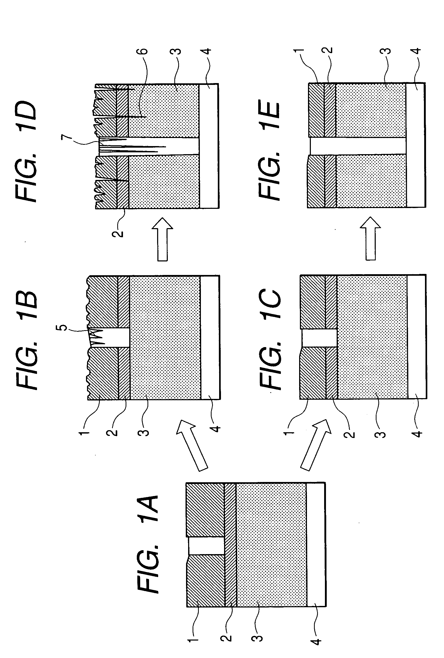
[0033]FIGS. 1A to 1E are cross sectional views to show a process of forming contact holes using as a mask a resist pattern formed by lithography with the use of an excimer laser as a light source. FIG. 1A shows an example of a sample to which the dry etching method of the present embodiment is applied. The film structure is composed of a resist 1 applicable to ArF lithography, an organic bottom-anti-reflection-coating (BARC) 2 that suppresses an abnormal pattern formation due to interference of laser reflection, a silicon oxide film 3 that is a film to be processed, and a base silicon substrate 4. Here, the film thickness of the resist applicable to the ArF lithography was set to 350 nm, and that of the BARC was set to 60 nm. It should be noted that an open portion at the center of the resist 1 in each of FIGS. 1A to 1E shows the inner wall of the contact hole.

[0034]FIGS. 1B and 1D are cross sectional views which show the result when a conventional etching pr...

second embodiment

[0047] Second Embodiment

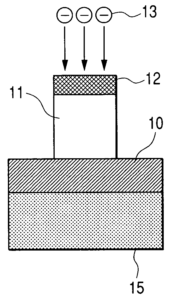
[0048] In this embodiment, resist modification and etching carried out in the same apparatus with the objective of reducing resist damage are exemplified. In general, resist modification is performed in a specifically designed modification apparatus, and then etching is performed in an etching apparatus. However, in the embodiment of the present invention, resist modification and etching are carried out by turns as shown by the steps of processing shown in FIGS. 5A to 5E. FIG. 5A is a cross sectional view before the processing, where an ArF resist 11, an anti-reflection coating 10, and a silicon oxide film 15 are laminated. FIGS. 5B and 5D depict resist modification cycles. A resist thickness 12 to be modified in one cycle of the resist modification is to be set larger than the resist thickness etched in the next etching cycle (FIGS. 5C and 5E). In this way, the resist surface is always modified at the time of etching, and resist damage can be reduced.

[0049]...

third embodiment

[0063] Third Embodiment

[0064] In this embodiment, a process in which the second embodiment and the first embodiment described above are combined together will be explained. First, the resist modification of the resist surface layer is carried out by using the method of the electron beam cure that was explained in conjunction with the second embodiment. In this case, the plasma gas used to generate electrons is a rare gas that does not form deposition radicals and reactive radicals. In this way, electrons are purely drawn toward the resist surface, and the resist modification effect can be enhanced. In the present embodiment, Ar was supplied at 50 ml / min, and the pressure was set to 2 Pa. During the resist modification cycle, 15,000 pulses of positive pulse bias were applied 50 msec after switching off the plasma. The electron acceleration voltage is about 100 V, and the dose amount is about 2,000° C. / cm2. The thickness of the resist modification is then about 10 to 20 nm. Subsequent...


PUM


Abstract

A condition without using Ar as plasma gas is applied to processing of an organic anti-reflection-coating, which suppresses a spatter effect and decreases the cleavage of C—H and OC—O bonds in a resist. As a result, roughness of the resist after processing the anti-reflection-coating can be suppressed, and pitting and striations after processing a next film to be processed, that is an insulating film, can be prevented. For a rare gas to be used at the time of processing the insulating film, any one of Xe, Kr, a mixed gas of Ar and Xe, and a mixed gas of Ar and Kr is applied in place of Ar, giving rise to reduction in pitting and striations after etching. In addition, a dry etching method with less critical-dimension shift and excellence in both apparatus cost and throughput can be provided by performing resist modification and etching by turns.

Description

CLAIM PRIORITY [0001] The present application claims priority from Japanese application JP 2003-303961, filed on Aug. 28, 2003, the content of which is hereby incorporated by reference into this application. FIELD OF THE INVENTION [0002] The present invention relates to a dry etching apparatus of the type used for etching an inter-layer-dielectric among dry etching processes and to a dry etching method; and, the present invention relates particularly to a method in which resist damage can be reduced in via etching, high-aspect-ratio contact etching, self-align-contact etching, trench etching, damascene etching, gate mask etching, and the like using a resist pattern for ArF lithography or later lithography. BACKGROUND OF THE INVENTION [0003] In a semiconductor device, the electrical connection between a transistor formed on a wafer and metal wiring and between metal wirings is established first by making contact holes on an inter-layer dielectric, that is formed on the upper part of ...

Claims


Application Information

Patent Timeline
IPC IPC(8): G03F7/40H01L21/027G03F7/11H01L21/28H01L21/3065H01L21/311H01L21/768
CPCH01L21/0275H01L21/0276H01L21/76802H01L21/31144H01L21/31116
Inventor NEGISHI, NOBUYUKIIZAWA, MASARUYOKOGAWA, KENETSU
Owner HITACHI HIGH-TECH CORP
Why Eureka
Try Eureka