Silicon photomultiplier tube
a technology of photomultiplier tube and silicon, which is applied in the direction of electron multiplier details, instruments, x/gamma/cosmic radiation measurement, etc., can solve the problems of inability to use an apparatus and relative cost, and achieve the effect of increasing the efficiency of short-wavelength light detection
- Summary
- Abstract
- Description
- Claims
- Application Information
AI Technical Summary
Benefits of technology
Problems solved by technology
Method used
Image
Examples
third embodiment
[0061]FIG. 4 is a graph showing the results of simulating the light detection efficiency of the silicon photomultiplier tube according to the present invention.
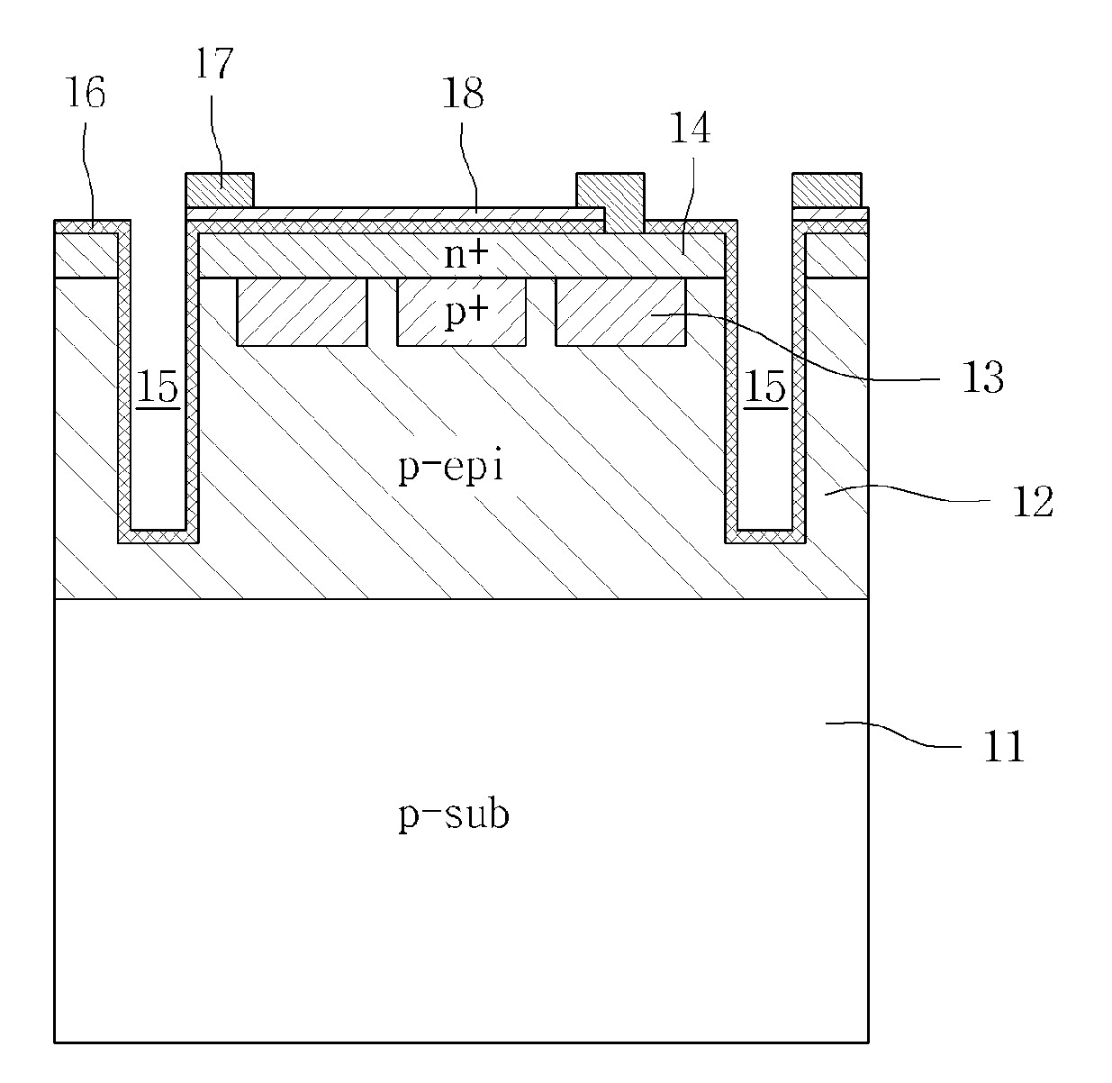
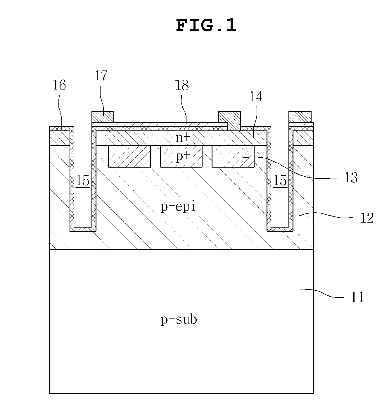
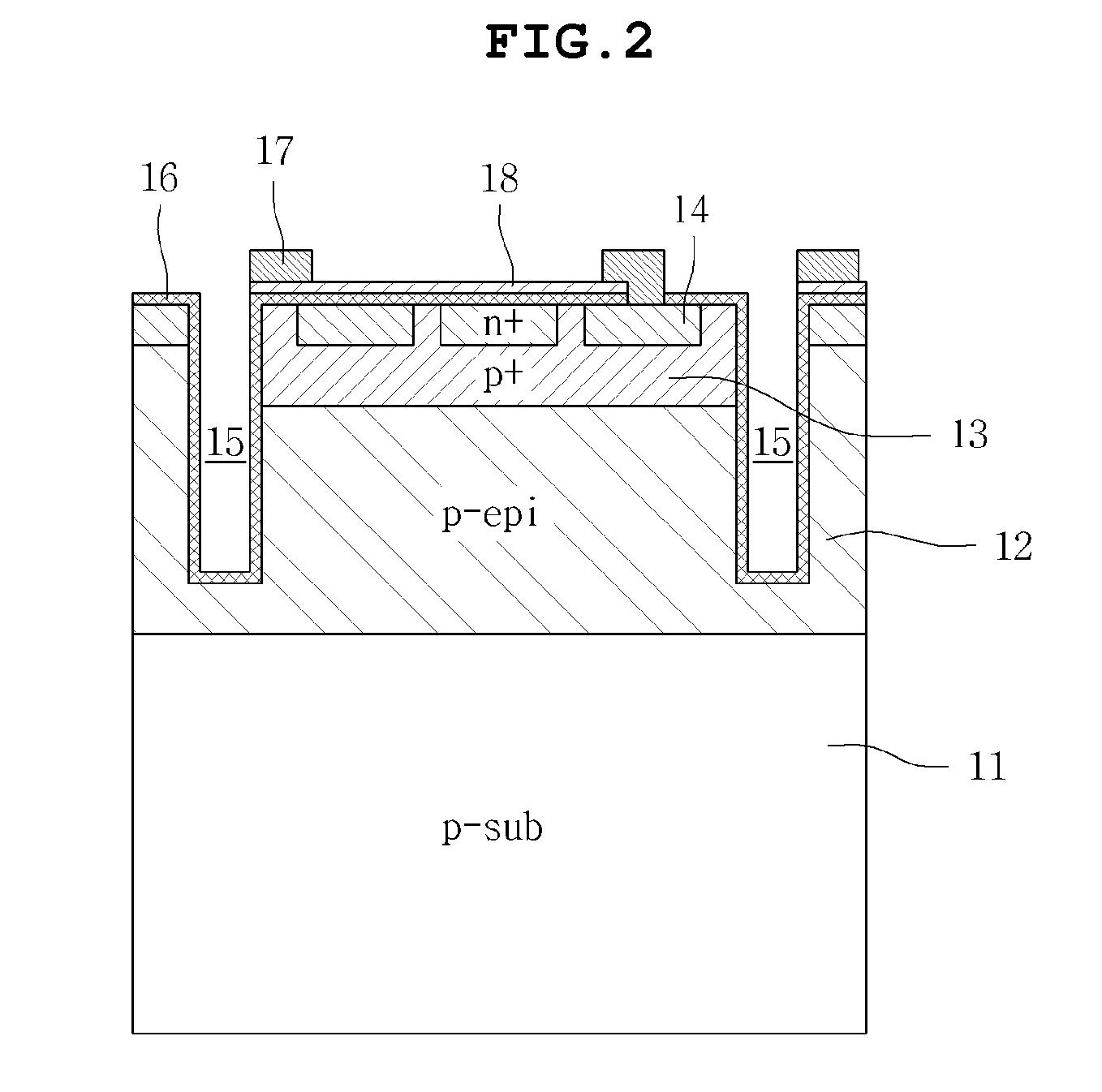
[0062]The silicon photomultiplier tube having the light detection efficiency shown in FIG. 4 is configured such that a dose of 3*1012 cm−3 is applied to the second type conductive layer 14, a dose of 2*1012 cm−3 is applied to the first type conductive layer 13, the first type epitaxial layer 12 has a doping agent concentration of 2*1015 cm−3, each cell has a width of 30 μm, and the width between adjacent rows in the first type conductive layer 13 formed in three rows is 0.5 μm. From FIG. 4, it can be seen that the light detection efficiency of this silicon photomultiplier tube to short-wavelength light having a wave length of about 500 nm is higher than that of the silicon photomultiplier tube including an integrally-formed first type conductive layer.
[0063]Since the silicon photomultiplier tube according to this embodiment...
fourth embodiment
[0065]As shown in FIG. 5, a silicon photomultiplier tube according to the present invention may further include guard rings 20 formed on the to outer walls of the separating elements 15.
[0066]These guard rings 20 are formed into second type guard rings 20 using an implant method after the formation of the separating elements, and each of the second type guard rings 20 has a doping agent concentration of 1014˜1018 cm−3. These guard rings 20, together with the separating elements 15 and the insulating material 19 charged in the separating elements 15, serves to prevent the photoelectrons generated from adjacent cells from infiltrating into the sensitivity region of other cells.
[0067]The guard rings 20 may be formed to partially surround the separating elements. As shown in FIG. 5, the guard rings 20 may be formed to surround the lower ends of the separating elements 15. However, this is only an example, and the guard rings 20 may be formed to partially surround the outer walls of the ...
PUM
 Abstract
Description
Claims
Application Information


