Capacitive load drive circuit and display device including the same

Inactive Publication Date: 2011-03-31
SHARP KK
View PDF14 Cites 5 Cited by
  • Summary
  • Abstract
  • Description
  • Claims
  • Application Information

AI Technical Summary

Benefits of technology

[0026]According to the first aspect of the present invention, by selectively operating the charge circuit and the discharge circuit included in the push-pull output unit, based on the result from comparing the input voltage and the output voltage to perform the charge and discharge of the capacitive load, the output voltage and the input voltage can be made equal. Moreover, selectively operating the charge circuit and the discharge circuit can prevent a steady current from flowing in the circuit, and thus, power consumption of the circuit can be reduced. Moreover, performing the charge and discharge of the capacitive load only when the output voltage is not equal to the input voltage can prevent wasteful power consumption by the charge and discharge of the capacitive load. Since in the second period, the output voltage is controlled to be equal to the input voltage, no circuit to retain the output voltage (e.g., a sampling gate) is required, by which an area and power consumption of the circuit can be reduced. For the voltage comparison unit, the drive control unit and the push-pull output unit, circuits robust against the process variation can be configured easily. Accordingly, a small-sized capacitive load drive circuit with low power consumption and robust against the process variation can be configured.
[0027]According to the second aspect of the present invention, by preferably controlling the states of the two switches, the voltage inputted to the comparison circuit is switched between in the first period and in the second period, and using the comparison circuit, the comparison result voltage in accordance with the comparison result between the input voltage in the first period and the output voltage in the second period can be found.
[0028]According to the third aspect of the present invention, in the comparison circuit including the capacitive element, the inverter circuit and the switch, by preferably controlling the state of the switch, the inverter circuit, in the second period, outputs the voltage in accordance with the voltage obtained by adding the inversion voltage of the inverter circuit (the input/output voltage when the input and the output

Problems solved by technology

The source driver circuit of the driver-integrated liquid crystal display device has problems that it has large power consumption, is susceptible to process variation, has a large circuit area, and the like.
When the operational amplifier in which the steady current flows is used, the power consumption of the source driver circuit increases.
Moreover, since an available common mode voltage in a differential amplifier circuit is limited, an operating voltage of the circuit needs to be made higher in order to exert desired performance while satisfying the limitation.
However, when the operating voltage is made higher, the power consum

Method used


Image

  • Capacitive load drive circuit and display device including the same
  • Capacitive load drive circuit and display device including the same
  • Capacitive load drive circuit and display device including the same

Examples


Embodiment Construction

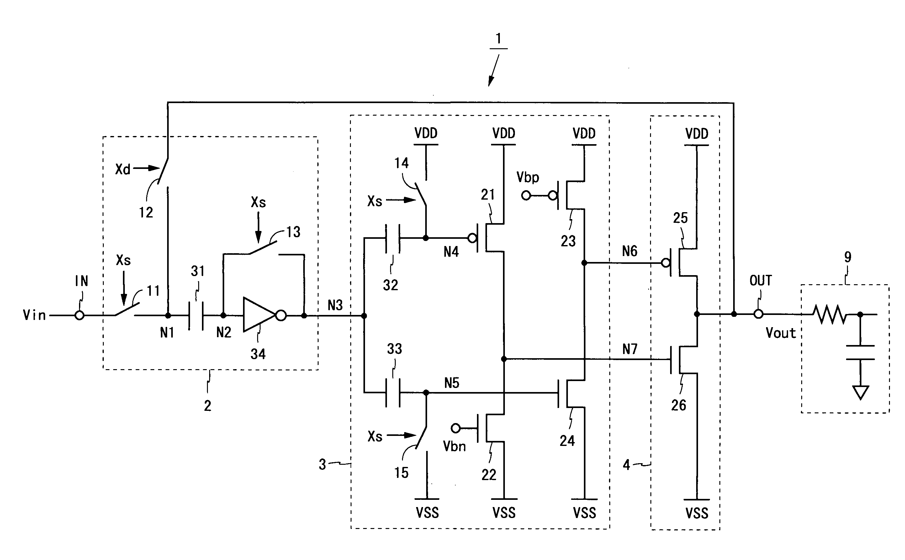
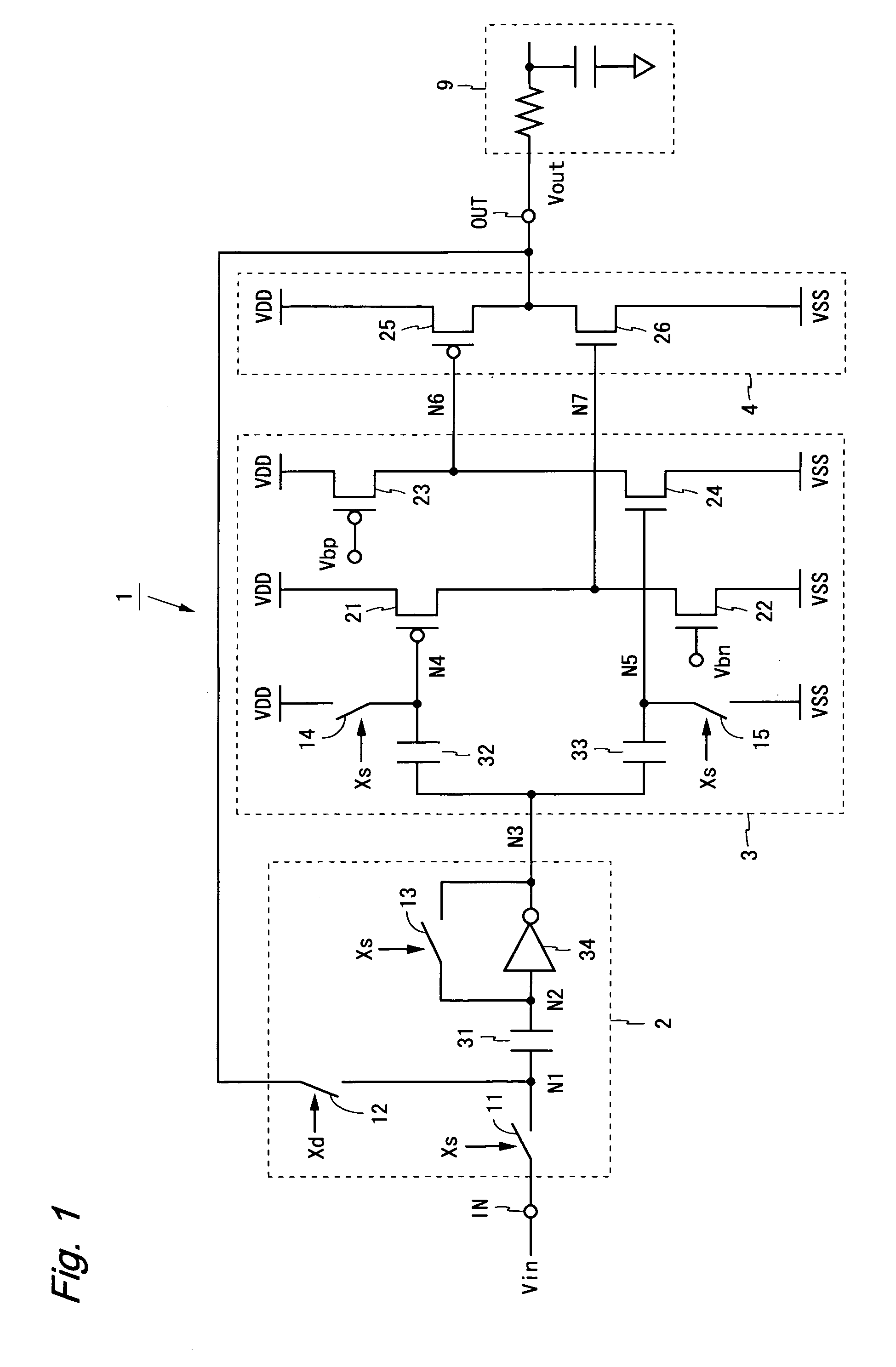
[0046]FIG. 1 is a circuit diagram of a push-pull type buffer circuit according to an embodiment of the present invention. A buffer circuit 1 shown in FIG. 1 is one specific example of a capacitive load drive circuit of the present invention, and drives a capacitive load 9 connected to an output terminal OUT, based on a voltage inputted from an input terminal IN. Hereinafter, the voltage inputted from the input terminal IN is referred to as an input voltage Vin, and a voltage outputted from the output terminal OUT is referred to as an output voltage Vout.

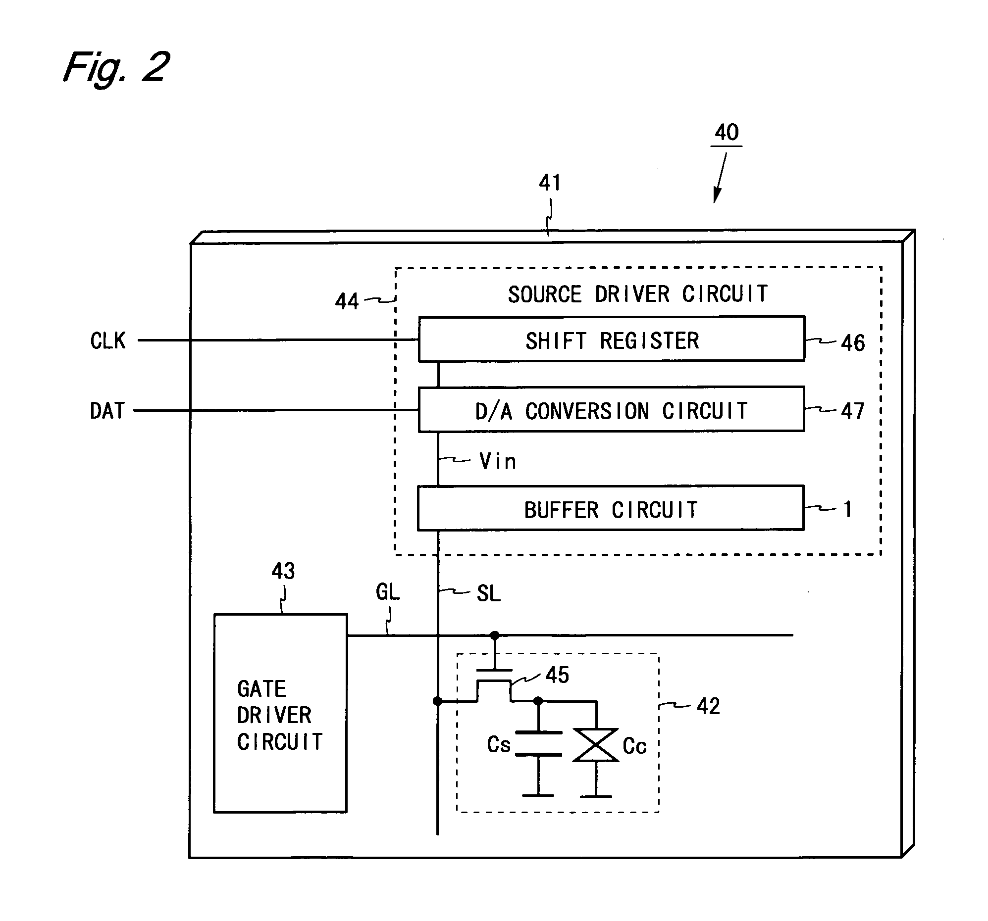
[0047]The buffer circuit 1 is used, for example, as an output stage circuit of a source driver circuit that drives a source line (also referred to as a data signal line, a video signal line or the like) in a driver-integrated liquid crystal display device (a liquid crystal display device in which pixel circuits and drive circuits thereof are integrally formed on the same substrate). FIG. 2 is a block diagram showing a configuration o...


PUM

PropertyMeasurementUnit
Electric potential / voltageaaaaaaaaaa
Power consumptionaaaaaaaaaa

Abstract

A buffer circuit drives a capacitive load based on a voltage Vin. In a setup period, switches are in an ON state, and in a drive period, a switch is in an ON state. A voltage comparison unit compares the voltage Vin in the setup period and a voltage Vout in a drive period to output a comparison result voltage. A push-pull output unit includes a TFT for charge and a TFT for discharge. A drive control unit controls the TFTs to be in an OFF state in the setup period, and in the drive period, selectively controls the TFTs to be in an ON state in accordance with the comparison result voltage. If Vout<Vin, the comparison result voltage rises, the TFT becomes in an ON state, a voltage at a node falls, the TFT becomes in the ON state, and the voltage Vout rises. Thus, there is a provided a small-sized capacitive load drive circuit with low power consumption and robust against process variation.

Description

TECHNICAL FIELD[0001]The present invention relates to a capacitive load drive circuit that drives a capacitive load based on an input voltage, and a display device including a capacitive load drive circuit.BACKGROUND ART[0002]As one of methods for downsizing a liquid crystal display device and reducing power consumption of the same, there has been known a method of integrally forming pixel circuits and drive circuits of the pixel circuits on a same substrate. Hereinafter, the liquid crystal display device configured by this method will be referred to as a “driver-integrated liquid crystal display device”. In the driver-integrated liquid crystal display device, the drive circuits are configured using thin film transistors (hereinafter, referred to as TFT (s)) made of low-temperature polysilicon, CG silicon (Continuous Grain silicon) or the like.[0003]FIG. 7 is a block diagram showing a configuration of a conventional driver-integrated liquid crystal display device. The liquid crystal...

Claims


Application Information

Patent Timeline
IPC IPC(8): G09G5/00H02J7/00
CPCG09G2310/027G09G3/3688
Inventor BROWN, CHRISTOPHEROGAWA, YASUYUKI
Owner SHARP KK
Why Eureka
Try Eureka