Method of manufacturing semiconductor device and substrate processing apparatus
- Summary
- Abstract
- Description
- Claims
- Application Information
AI Technical Summary
Benefits of technology
Problems solved by technology
Method used
Image

Examples
examples
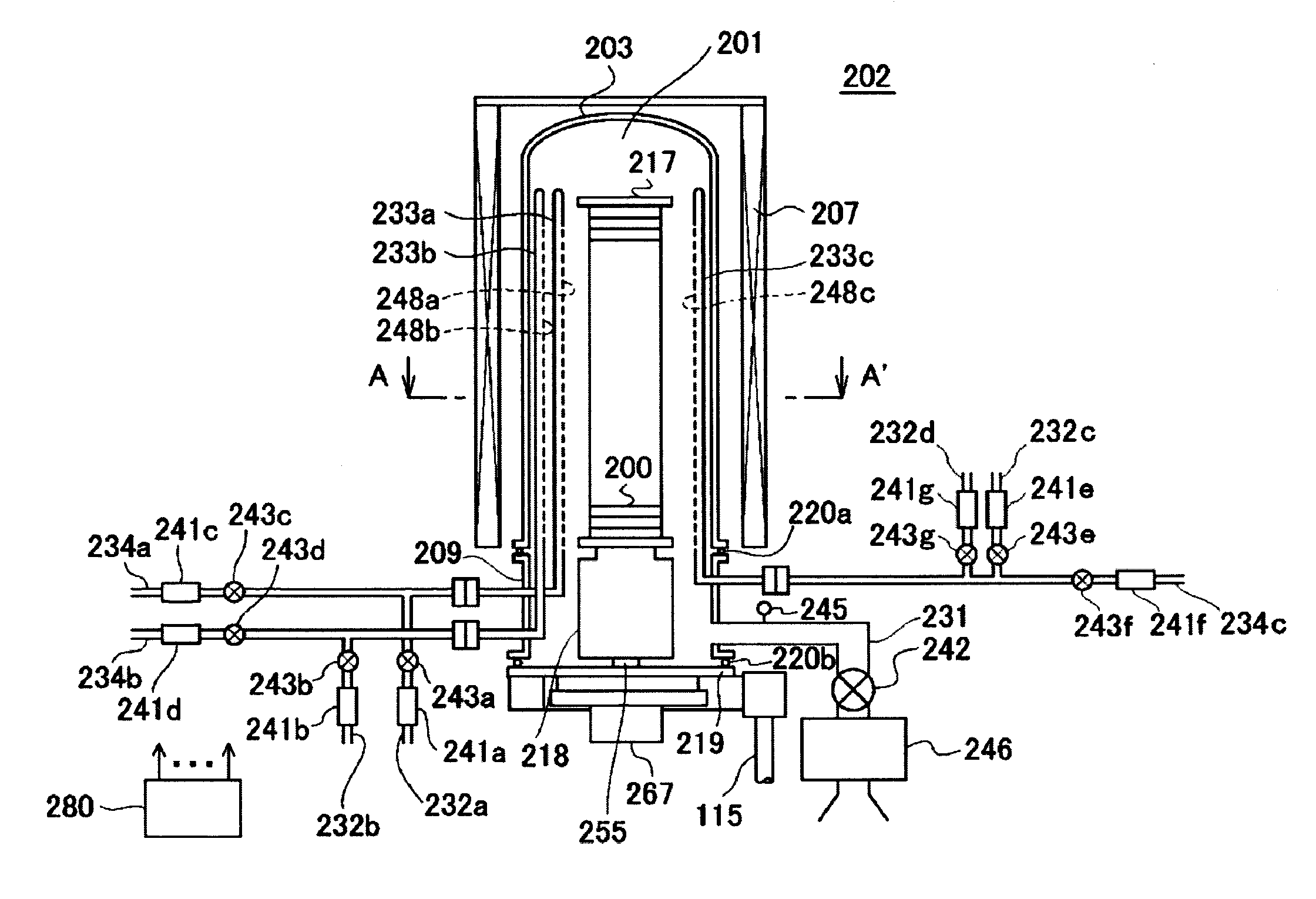
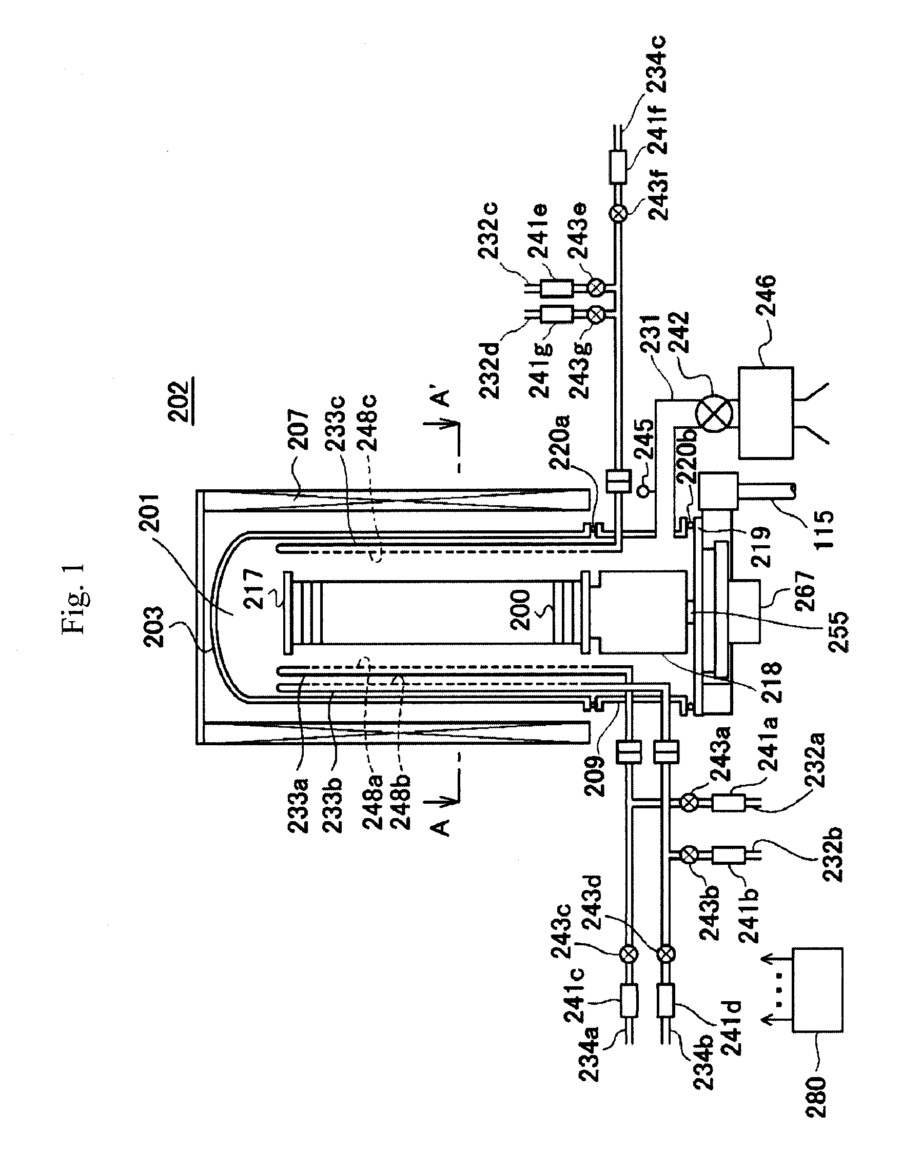
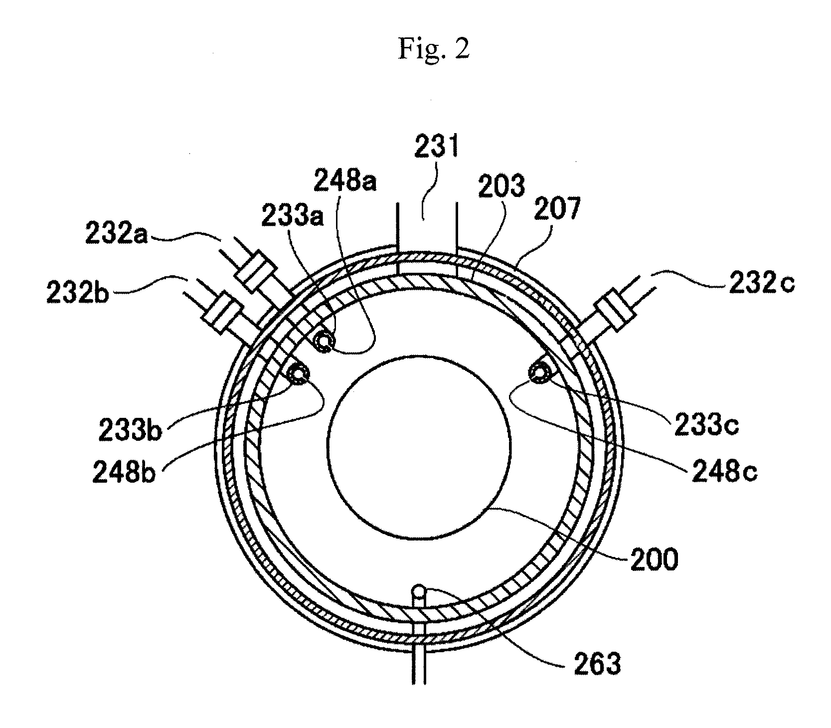
[0148]Silicon oxide films were formed on wafers according to the film-forming sequence of the embodiment of FIG. 4, and film growth rates (SiO film growth rates) and film thickness uniformities in surfaces of the wafers (SiO film thickness uniformities) were measured. Except for the flow rates of HCD and DCS, film-forming conditions (process conditions in each step) were set in the process condition ranges described in the previous embodiments. The flow rate of DCS was kept at a value in the range from 1 slm to 2 slm, the flow rate of HCD was varied in the range from 0 slm to 0.2 slm, and the flow rate ratio of HCD / DCS was varied among (A) 0%, (B) 3%, (C) 6%, and (D) 10%. Hereinafter, these will be referred to as a flow rate condition (A), a flow rate condition (B), a flow rate condition (C), and a flow rate condition (D). The HCD / DCS flow rate ratio at the flow rate condition (A) 0% means the case where HCD was not added to DCS (the case where only DCS was supplied). Furthermore, i...
PUM
| Property | Measurement | Unit |
|---|---|---|
| Fraction | aaaaa | aaaaa |
| Fraction | aaaaa | aaaaa |
| Fraction | aaaaa | aaaaa |
Abstract
Description
Claims
Application Information
 - R&D
- Intellectual Property
- Life Sciences
- Materials
- Tech Scout
- Unparalleled Data Quality
- Higher Quality Content
- 60% Fewer Hallucinations
Browse by: Latest US Patents, China's latest patents, Technical Efficacy Thesaurus, Application Domain, Technology Topic, Popular Technical Reports.
© 2025 PatSnap. All rights reserved.Legal|Privacy policy|Modern Slavery Act Transparency Statement|Sitemap|About US| Contact US: help@patsnap.com