
Growth method for high-speed and high-quality monocrystal diamond

A single crystal diamond and growth method technology, applied in the growth of high-quality single crystal diamond, epitaxial growth of single crystal diamond material, high-speed field, can solve the problem of many defects, low growth efficiency of single crystal diamond, unfavorable diamond development, and slow diamond growth rate and other issues to achieve the effect of high-speed growth

Active Publication Date: 2018-10-02
INST OF SEMICONDUCTORS - CHINESE ACAD OF SCI +1
View PDF4 Cites 2 Cited by
  • Summary
  • Abstract
  • Description
  • Claims
  • Application Information

AI Technical Summary

Problems solved by technology

However, in the growth process of single crystal diamond, when the growth rate of the diamond epitaxial layer is relatively high, the obtained diamond epitaxial layer often has problems such as poor quality, many defects, and poor optical and electrical properties; The growth rate is generally relatively slow, which leads to the low growth efficiency of high-quality single crystal diamond, which is not conducive to the development of diamond. Therefore, it is necessary to propose a new method to solve the problem of high-speed, high-quality growth of diamond.

Method used


Image

  • Growth method for high-speed and high-quality monocrystal diamond
  • Growth method for high-speed and high-quality monocrystal diamond
  • Growth method for high-speed and high-quality monocrystal diamond

Examples


Embodiment

[0035] Step 11: The substrate is diamond, and the angle between the substrate and the (100) plane is 2°.

[0036] Step 12: cleaning the substrate, and finally drying the substrate with nitrogen.

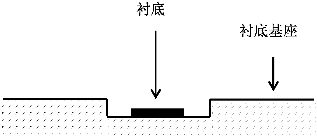
[0037] Step 13: The substrate base adopts a groove structure, and the substrate surface is 0.5 mm away from the substrate base surface.

[0038] Step 14: substrate plasma etching, the etching conditions are: etching time is 30min, the etching conditions are microwave power 5kW, air pressure 120torr, hydrogen flow rate 500sccm, and substrate etching temperature 850°C.

[0039] Step 15: The growth parameters used for high-speed growth of the diamond support layer are as follows: microwave power 5kW, growth pressure 240torr, hydrogen flow 500sccm, methane concentration 10%, growth temperature 1150°C, growth time 6h.

[0040] Step 16: Perform plasma etching on the surface of the diamond support layer, etching conditions: etching time is 60 minutes, etching conditions are microwave power...


PUM

PropertyMeasurementUnit
thicknessaaaaaaaaaa

Abstract

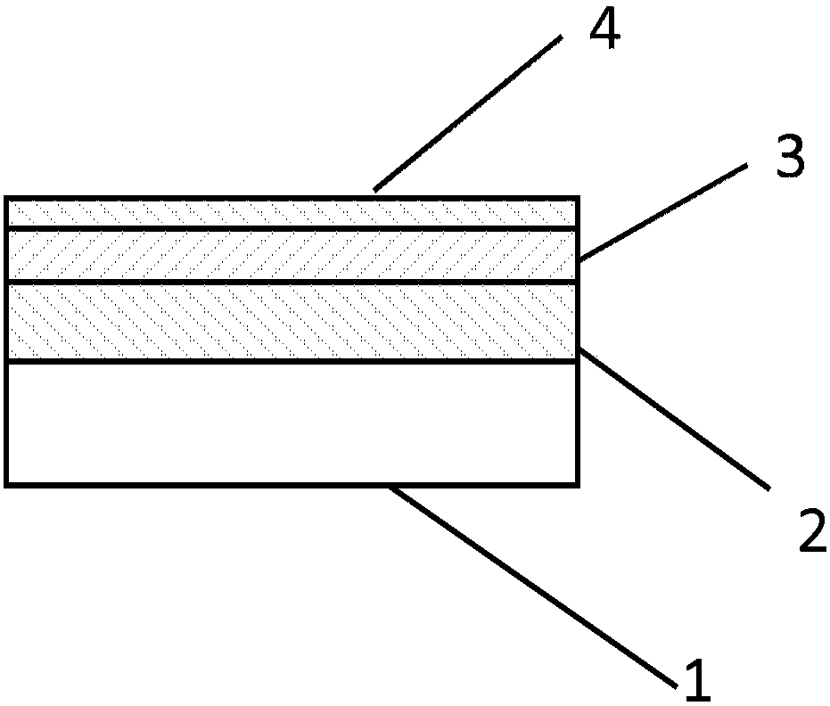
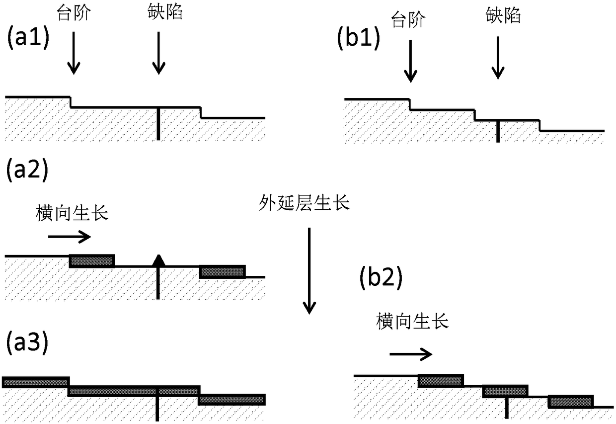
The invention discloses a growth method for a high-speed and high-quality monocrystal diamond. The method comprises the following steps: growing a diamond supporting layer on the surface of a substrate; growing an intermediate defect barrier layer on the surface of the diamond supporting layer; growing a diamond surface layer on the surface of the intermediate defect barrier layer. The method is characterized in that a layer of thick diamond supporting layer grows on the substrate at higher growth rate; the intermediate defect barrier layer grows on the diamond supporting layer and prevents defects in the diamond from extending towards the surface by adopting a step growth mode; the diamond surface layer grows on the intermediate defect barrier layer; the high-quality diamond surface layeris obtained at lower growth rate by adopting optimized growth conditions. According to the growth method, the high-quality monocrystal diamond grows by adopting a three-layer structure. According tothe growth method disclosed by the invention, the problem of contradiction between high growth rate and quality of an epitaxial layer in the traditional diamond growth process is solved.

Description

technical field [0001] The invention relates to the technical field of thin film and crystal growth, relates to a single crystal diamond material epitaxial growth method, in particular to a high-speed, high-quality single crystal diamond growth method. Background technique [0002] Semiconductor diamond is an excellent semiconductor material with a wide band gap, high room temperature electron and hole mobility, high breakdown electric field strength, high thermal conductivity and relatively low dielectric Constant, can be said to be the ultimate semiconductor. The excellent properties of semiconductor diamond make it have great application potential in high-temperature, high-frequency, high-power electronic devices and deep ultraviolet light-emitting diodes and detectors. At the same time, it can also be applied to electrochemical and biosensors and solid-state quantum computing. [0003] Diamond devices that have been prepared so far include Schottky barrier diodes, field...

Claims


Application Information

Patent Timeline
Patent Type & Authority Applications(China)
IPC IPC(8): C30B29/04C30B25/20
CPCC30B25/205C30B29/04
Inventor 龚猛周广迪郁万成金鹏王占国
Owner INST OF SEMICONDUCTORS - CHINESE ACAD OF SCI
Learn More